SEMICONDUCTOR INDUSTRY
UPDATE
April 2019
McIlvaine Company
Presto Engineering Upgrades Semiconductor Testing
Facility
Intel
to Ramp
Up 14nm Production
Seeking to allay fears of revenue shortfall amid tight supply, Intel said Friday
that the company believes it has the supply to meet its full-year sales target
of $69.5 billion. The company also reiterated plans to increase its capital
spending for the year to a record $15 billion and to be in volume production of
10nm chips next year.
In an open letter published on Intel's website Friday, Bob Swann, Intel's
interim CEO, said the company increased capital spending includes an additional
$1 billion to be spent on increasing 14nm capacity at Intel Fabs in Oregon,
Arizona, Ireland and Israel. Swann said the increased spending and other
efficiencies is increasing Intel's supply to respond to customer demand.
The strength of the PC market — which Intel now expects to grow for the first
time since 2011 — has put pressure
on the company's network of fabs, Swann said. Intel is prioritizing the
production of Xeon and Core processors to serve the high-performance computing
segments of the market, Swann said.
"That said, supply is undoubtedly tight, particularly at the entry-level of the
PC market," Swann said.
In an email exchange with EE Times, Intel declined to provide further details
beyond what is in Swann's letter.
Patrick Moorhead, president and principal analyst at Moor Insights & Strategy,
said he was not surprised by the letter, saying he had heard rumblings in the
supply chain. "While I am sure Intel would want to have 10nm online now, most of
the current challenges stem from upside demand for 14nm parts," Moorhead said.
"Every market is up — even PCs — which is putting a strain on 14nm. Moving
notebook parts from two to four cores I am sure contributed to the upside
challenges, but [are] not the primary reason."
Intel has for months been struggling to ramp up its 10nm process technology with
adequate yields. The company was initially expected to be in volume production
on 10nm by the end of this year, but said earlier this year it was pushing 10nm
out to 2019. Intel's struggles with 10nm have led to speculation that the
company is in danger of losing market share in the resurgent PC processor market
to archrival AMD.
"The challenges that Intel is having regarding their execution on delivering
their next generation technology could not have come at a more inopportune
time," said Len Jelinek, senior director for semiconductor manufacturing with
IHS Markit. "Intel delivery issues
are providing an opportunity for their competition, AMD, to gain market share in
a highly competitive market."
Jelinek said multiple competitors could be posed to gain market share in areas
outside PCs and gaming if Intel's struggles with 10nm continue into 2019.
Quoting market research from Gartner, Swann said second quarter PC shipments
increased for the first time in six years. Intel expects to total PC market to
grow modestly this year, driven by strong demand for gaming and commercial
systems, Swann said.
In recent weeks, whispers of an Intel processor shortage have led to concern
about the effect on the PC market and the memory chip market. Earlier this
month, TrendForce, a market research firm that tracks memory chip pricing,
reported that a shortage of Intel processors would hamper notebook shipments and
exacerbate memory pricing declines.
TrendForce reported that PC OEMs were reporting an insufficient supply of
processor based on Intel's Whiskey Lake platform. Whiskey Lake is the codename
for Intel's third refinement to the 14nm Skylake microarchitecture and includes
version of Core i7, Core i5 and Core i3, all of which were launched in the third
quarter.
Presto Engineering Upgrades Semiconductor
Testing Facility
Semiconductors play increasingly important control roles in automotive,
industrial and safety critical applications. Quality and reliability are
therefore of vital importance and so Presto Engineering has completed
certification to the ISO 9001:2015 quality standard at its facility in Caen,
France, which is Europe’s largest independent semiconductor test facility
“We have an extensive and comprehensive range of semiconductor test equipment,”
said Dr Alban Colder, Presto’s Site Director at Caen. “This includes testing at
every stage from wafer, through die, to final packed device. As part of the ISO
9001: 2015 quality standard, we have a comprehensive range of equipment for
non-destructive analysis such as X-Ray to check packaging and bondings, and
ultrasound to see inside a device to check for delamination, voids and cracked
silicon. There is also equipment to check for failure localization by
photoemission or thermal laser stimulation, and deep physical analysis, i.e.
strip a device down layer by layer to see exactly where it is failing and why.
Other advanced equipment such as an atomic force microscope or a scanning
electron microscope are used to reveal the precise details of the structure of a
chip down to a few nanometers.”
The key part of a quality system in semiconductors industry, is traceability.
Detailed record keeping traces every wafer, every operation, every die and every
test. Thus, in the event that there is a faulty chip in the field, it can be
traced back to try and determine the cause and to see if any other chips have
been affected that might necessitate a recall. In the case of an automotive
recall, this could be very expensive, so it is vital to be able to narrow the
problem down to only the affected chips.
Martin Kingdon, Presto’s VP of Sales, added, “We have assembled a suite of
state-of-the-art equipment as part of our commitment of quality and this new
standard. We provide customers with a comprehensive service once they provide us
with a design that covers every stage of the chip manufacturing and testing
process right through to final product. As part of our quality assurance to
customers, we rigorously test at every stage. Such a comprehensive test and
failure analysis capability all together under one roof is very rare; usually it
requires a number of different test houses which means that issues could be
missed. Having all the skills and equipment together in one place means that we
can keep searching until we find the cause of a problem so that it can be
resolved, and quality maintained.”
About Presto Engineering:
Presto Engineering provides outsourced operations for semiconductor and IoT
device companies, helping its customers minimize overhead, reduce risk and
accelerate time-to-market. The company is a recognized expert in the development
of industrial solutions for RF, analog, mixed-signal and secured applications –
from tape-out to delivery of finished goods. Presto’s proprietary, highly secure
manufacturing and provisioning solution, coupled with extensive back-end
expertise, gives its customers a competitive advantage. The company offers a
global, flexible, dedicated framework with operations across Europe, the USA and
Asia. For more information, visit: www.presto-eng.com or email
info@presto-eng.com
TSMC taped out its first chip in a process making limited use of extreme
ultraviolet lithography and will start risk production in April on a 5-nm node
with full EUV. Separately, the foundry forged partnerships with four partners to
support online services for back-end chip design.
The foundry’s update showed that area and power gains continue in its
leading-edge nodes, but chip speeds are no longer advancing at their historic
rate. To compensate, TSMC gave an update on a half-dozen packaging techniques
that it is developing to speed connections between chips.
Backers say that cloud-based services will shorten the time and extend the reach
of chip design tools, helping expand a semiconductor industry facing the
slowdown of Moore’s Law. However, they note that cloud design is still in an
early phase that typically requires setting up and optimizing custom sites.
In process technology, TSMC announced that it taped out a customer chip in an
N7+ node that can use EUV on up to four layers. Its N5 that will use EUV on up
to 14 layers will be ready for risk production in April. EUV aims to lower costs
by reducing the number of masks required for leading-edge designs.
Rival Samsung is ramping a 7-nm node using EUV. Intel is not expected to use EUV
anytime soon, according to analysts. Globalfoundries announced in August that it
has halted work on 7 nm and EUV.
TSMC said that N5 will deliver 14.7% to 17.7% speed gains and 1.8 to 1.86 area
shrinks based on tests with Arm A72 cores. The N7+ node can deliver 6% to 12%
less power and 20% better density; however, TSMC did not mention speed gains.
Chip designs for the N5 node can start today, although most EDA tools won’t hit
a 0.9-version readiness until November. Many of TSMC’s foundation IP blocks are
ready for N5, but some, including PCIe Gen 4 and USB 3.1, may not be ready until
June.
The N7+ node sports a tighter metal pitch and includes a single-fin library that
can help lower dynamic power. It will be available in a version for automotive
designs by April. N7+ offers “nearly the same analog performance as N7,” said
Cliff Hou, vice president of technology development at TSMC.
Transistor density at N7 is 16.8x greater than at the foundry’s 40-nm node, said
TSMC. Unfortunately, costs are increasing, too. One source pegged total costs
for an N5 design including labor and licensing at $200 to $250 million, up from
$150 million for a 7-nm chip today, limiting pursuit of Moore’s Law to the
well-heeled.
Separately, TSMC offers two flavors of a planar 22-nm process. It aims to
compete with fully depleted silicon-on-insular processes from Globalfoundries
and Samsung. GF announced late last month that it has more than 50 design wins
for its 22-nm version of FD-SOI.
Engineers can start designs before the end of the year on TSMC’s 22ULP and ULL
processes that generally use 28-nm design rules and support 0.8 to 0.9 V. Some
IP will not be available for the 22-nm nodes until June, including PCIe Gen 4,
DDR4, LPDDR4, HDMI 2.1, and USB 3.1 blocks.
The ULP version is focused on performance and offers up to 10% speed gains or
20% less power and a 10% shrink over its 28 HPC+. The ULL version, about a
quarter behind in readiness, aims at lowest power for designs such as Bluetooth
chips. By April, a version will be ready supporting voltages from 1.05 to 0.54 V
with more optimization for analog circuits.
In packaging, Hou gave updates on two of TSMC’s four wafer-level fan-out options
used, for example, to link as smartphone application processors and memory.
InFO-on-Substrate is a chip-first process using two-micron interconnects between
SoCs and 40-nm SoC I/O pitches. It has been qualified on 65-mm2 chips now in
production. The foundry aims to expand it to components at 1.5x reticle size.
InFO-Memory-on-Substrate will be qualified for production by the end of the
year. It can link logic and typically HBM memory on a full reticle 830-mm2
device.
The 2.5D process that TSMC calls CoWoS will shrink from using a 180- to
150-micron C4 bump pitch now to 130-micron pitches by the end of the year. It
will expand from 1.5x reticle to 2x reticle by April to support a class of
designs such as large GPUs and some networking ASICs.
Yet another category, called System-on-Integrated-Chips (SoIC), will have EDA
support and foundry qualification for starting designs before May. The approach
puts one or two chips on top of another using through silicon vias connecting
bumps with a pitch of less than 10 microns. “It’s another way to lift
performance and memory bandwidth,” said Hou.
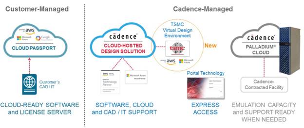
Separately, TSMC announced that it has worked with Amazon Web Services, Cadence,
Microsoft Azure, and Synopsys to enable back-end chip design based in the cloud.
The so-called Virtual Design Environment will initially use “storefronts”
created by Cadence and Synopsys to support digital RTL-to-GDSII and custom
schematic-capture-to-GDSII flows.
TSMC expects that other EDA vendors will eventually join the effort that also
will come to include front-end design flows. To test out the capabilities, TSMC
is designing its N5 SRAM using the service. In addition, Synopsys used it to
tape out a PCIe Gen 5 PHY block in TSMC’s 7-nm node, and startup SiFive used it
to design a 28-nm RISC-V core.
“We haven’t tested all the possible combinations, but given that our PDKs are
certified, we’re confident in the service,” said Suk Lee, a senior director of
design infrastructure marketing at TSMC, noting that executives agreed to create
the service just six months ago. “We did our N5 SRAM development in the cloud,
and that speaks to how comfortable we are.”
Initially, customers need to engage one of the partners to create a custom site
for them based on user requirements and license agreements. Partners declined to
comment on liability for any IP theft, likely an element of those business
agreements.
“There is a setup time involved,” said Naveed Sherwani, chief executive of
SiFive, which taped out a test device based on its 64-bit Freedom Unleashed 540
chip. “You have to set up chambers [hosted by online sites] and NDAs and
business things … [eventually,] cloud business processes have to move more at
the speed of the cloud … with [fewer] meetings.”
Sherwani and others foresee potential for a future portal that leads an engineer
through a process of licensing and configuring a service for any design. “We are
taking the first baby steps in this direction, but we have a ways to go,” he
said.
For best response times, SiFive set up separate sites hosted by regional data
centers for its teams in Silicon Valley and Bangalore. “We completed a whole
front- and back-end design in less than three months, which is a record,” he
said.
The SiFive project did not involve a commercial SoC with license chains, so
Sherwani had no evaluation of the costs of online design. Those costs will
depend, in part, on the kinds of CPU and storage configurations that engineers
choose, itself a complex area where hosts such as AWS and Microsoft’s Azure
service compete.
For example, Amazon provides what it calls an EC2 z1d instance with sustained
4-GHz frequency on an Intel Skylake-class Xeon. It is geared, in part, to let
chip designers put more work on a single CPU, reducing the cost of per-CPU EDA
licensing.
Despite the hurdles still ahead, “we are committed to put all of our low- and
medium-end designs in the cloud,” starting with cores and moving to sensor and
IoT and more complex SoC designs next year, said Sherwani.
“The very high-end won’t move to cloud anytime soon … very complex server-class
designs have 300-person teams, and they don’t need that class of support,” given
the complexity and low volume of such designs, he added.
Cadence positions the new TSMC offering as one part of its cloud portfolio.
(Source: Cadence)
Online design is not new. NXP published
a whitepaper in 2012
about its use of AWS for chip design. The new wrinkle is EDA, and foundry
providers are now ramping up their own managed services on cloud platforms.
Cadence said that it has “experience hosting design environments for more than
100 customers,” as part of TSMC’s announcement. Synopsys said that it, too, has
done such work for several years.
At last year’s Design Automation Conference, Cadence made a big push for
providing its tools online. However, analysts said that they expect
EDA to move slowly to the
cloud.
In any industry, cloud users typically move existing processes online and then
customize them, said Kushagra Vaid, general manager for Microsoft’s Azure
service. A former chip designer, Vaid said that he has talked to small, medium,
and large chip companies embracing cloud services.
“It’s underway now, being [optimized] for the back end, and the front end will
go through the same process — this is a watershed moment for semiconductors,”
said Vaid in an interview.
In a keynote, he made the case for online design given that IT departments can
keep up with infrastructure investments from the likes of AWS and Azure.
For example, Microsoft spends a billion dollars a year on security, including
everything from fences to appliances and programs for its network of more than a
hundred data centers with a total of more than a million servers.
Just when other EDA vendors, such as Mentor Graphics, jump in is unclear. A
spokesman for MathWorks said that its online offering is gaining popularity with
academics and customers who are moving other jobs to the cloud.
“We believe that the vast majority of our product use is still on company-owned
hardware; however, interest in using our products in the cloud for IoT, training
deep-learning networks, and large-scale simulations has been rising quickly over
the last 18 months,” said a company spokesman.
“Security used to be the reason that our customers would not move to the cloud,
but now it is increasingly becoming a reason for their move,” he said.
— Rick Merritt, Silicon Valley Bureau Chief, EE Times
McIlvaine Company
Northfield, IL 60093-2743
Tel:
847-784-0012; Fax:
847-784-0061
E-mail:
editor@mcilvainecompany.com
Web site:
www.mcilvainecompany.com