SEMICONDUCTOR INDUSTRY
UPDATE
October 2018
McIlvaine Company
Advanced Manufacturer to Set Up at University of Adelaide
SK Hynix Achieves Record-High Q2 Profit On Strong DRAM, NAND
Growth
The Australian-based Silanna Group is setting up a high-tech advanced
manufacturing research facility on the University of Adelaide campus.
Silanna Group is partnering with the University of Adelaide to bring new
research capability to the state, developing world-leading products through the
engineering of new and innovative semiconductor technology.
The first stage of the partnership is the establishment of the state-of-the-art
‘picoFAB’ facility within the University’s Faculty of Engineering, Computer and
Mathematical Sciences.
The first of its kind in South Australia, this facility is designed to engineer
new semiconductor materials at the atomic level, using novel materials and
unique techniques.
University of Adelaide Vice-Chancellor and President Professor Peter Rathjen
says: “This is not just an investment in a new facility at the University of
Adelaide, it is the kind of investment in innovation, global connectivity and
graduate skills that South Australia needs.
“It is a perfect example of how the University can bring together its
outstanding research expertise, its unique facilities, its students and
connections to attract global industry to Adelaide.”
This new facility will drive Silanna’s advanced compound semiconductor research
program. At its heart is a new US$6.5 million tool that grows the new
crystalline materials, atomic layer by atomic layer. The ‘Molecular Beam
Epitaxy’ tool has been purpose-built by international technology company Veeco
Instruments Inc.
Silanna has a track record in demonstrating new semiconductor technologies and
commercialization. The establishment of the picoFAB will add to the University’s
diverse materials research programs, as well as the state’s growing advanced
manufacturing industry.
Silanna’s products are used in the communications, defense, medical and space
industries, including new types of solar cells, antennas for mobile phones,
power switches and light-emitting diodes.
Silanna’s Chief Scientist, Dr. Petar Atanackovic, is South Australian and a
University of Adelaide graduate. After graduation he took his skills to
California’s Silicon Valley and Stanford University. He founded Translucent, a
unique materials start-up in Palo Alto and, upon returning to Australia, went on
to develop commercial scale Gallium Aluminum Nitride semiconductors.
“I wanted to help create the same opportunities I had in Silicon Valley at the
University of Adelaide,” says Dr. Atanackovic. “The University has some unique
capabilities on campus with research and training programs that are
complementary to our operations, and access to a whole generation of potential
young ‘quantum mechanics’ as future employees.
“Together with the new high-tech ecosystem that’s developing in Adelaide, and
Adelaide’s lifestyle and culture as a center of learning, there are clear
drawcards to overseas professions and businesses wanting to establish themselves
and take advantage of the opportunities that are here. Adelaide is very similar
to Santa Barbara about 30 years ago. If there is a high-technology industry
here, they will come.”
South Australian Minister for Industry and Skills the Hon. David Pisoni says:
“The new partnership between the University of Adelaide and Silanna Group is a
great example of industry and researchers working together to develop new
commercial solutions and drive innovation—collaborations that we want to see
more of in South Australia.
“Silanna’s new facility adds advanced manufacturing capabilities in South
Australia that will attract further investment into our state. Importantly, it
will provide STEM students with access to world class infrastructure that will
give them practical experience and further their employment opportunities in
their home state.”
Faculty of Engineering, Computer and Mathematical Sciences Executive Dean
Professor Anton Middelberg says: “This partnership gives our students and staff
the opportunity to engineer the cutting edge of science, in areas of future
jobs.
“Having Silanna in our Faculty means our students will be interacting with
industry researchers and global leaders in materials engineering for a great
educational experience.”
A video about this facility can be seen at https://youtu.be/ELEoItOKH00.
SK Hynix to Build New Plant in Icheon
SK Hynix Inc. said it will build a new semiconductor fabrication (FAB) plant at
its headquarters in Icheon, southeast of Seoul, seeking to cope with the rising
demand for memory chips around the globe.
South Korea's No. 2 chipmaker said the construction will begin later this year,
which will be completed in October 2020. The combined size of the project is
estimated at 3.5 trillion won (US$3.1 million).
The company said it has not yet set the production portfolio of the new plant,
claiming it is subject to change depending on market environments and its
technology progress throughout 2020.
SK Hynix said the new factory is anticipated to generate an economic effect of a
whopping 80.2 trillion won and create jobs for around 348,000 people.
The company did not provide details behind the calculation but claimed that the
new plant will lend support to the South Korean economy, as well as the chip
industry as a whole.
SK Hynix said the demand for memory chips will continue to rise down the road
especially from the server and mobile segments, along with the increasing
presence new technologies such as artificial intelligence.
The company said it is inevitable for the company to make investments in
expanding its production facilities to cope with the trend.
"This new FAB in Icheon is a third FAB setup after the M14, which was completed
in 2015, and another FAB in Cheongju, which is under construction," the company
said. "After the construction of the new FAB is completed and equipment wholly
installed, the total investment in the three FABs will even exceed 46 trillion
won.
"SK Hynix will continue to make efforts to solidify its industry leadership, as
well as to contribute to the national economy and social value creation."
SK Hynix Achieves Record-High Q2 Profit On Strong DRAM, NAND
Growth
SK Hynix, South Korea’s second-largest memory chip provider, achieved the
largest-ever second-quarter profit this year, owing to unwavering growth of
demand for memory chips.
The firm is forecast to continue benefiting from favorable market conditions in
the second half of the year, according to its earnings announcement.
The Korean memory chip maker posted 10.37 trillion won ($9.25 billion) in sales
and 5.57 trillion won in operating profit for the April-June period, jumping 55
percent and 83 percent respectively from a year earlier.
The second-quarter net profit stood at 4.33 trillion won, surging 75 percent
from the same quarter last year.
All figures marked all-time highs boosted by favorable market conditions, the
company said.
The bit shipments of DRAM increased 16 percent from the previous quarter because
of the robust server and PC DRAM markets, and NAND flash bit shipments expanded
19 percent due to growing SSD demand and a rising trend of NAND density in
Chinese mobile phones.
A 4 percent increase in the average selling price of DRAM products on-quarter
contributed to the record profit in the second quarter. The average selling
price of NAND flash products, on the other hand, fell 9 percent.
For the next six months, market demand for DRAM is expected to show steady
growth due to the expansion of investments by US and Chinese businesses into
internet data centers. Supply is estimated to be far short of the growth in
demand because of limited growth of production due to technological difficulties
for nano-process.
“SK Hynix will place its focus on expanding leading-edge technologies to mass
production to respond to the market demand,” said Lee Myoung-young, executive
vice president at SK Hynix.
“It will consistently expand the portion of 1Xnm mainly in the sales of server
and mobile DRAM, which are expected to have strong demand growth,” he said. “The
portion of the 1Xnm will be expanded from around 20 percent as of the second
quarter to 33 percent by the end of the year.”
The next generation of 1Xnm, 1Ynm process will be applied for mass production,
starting next year.
The company also plans to stretch its cutting-edge 72-Layer 3D NAND and make
efforts to smoothly supply high-density mobile solutions and enterprise SSDs.
Meanwhile, the company aims to complete the cleanroom construction of a new fab
in Cheongju, North Chungcheong Province, by the end of this September, and hopes
the fab will contribute to its production capacity from the beginning of next
year.
In addition, the cleanroom space expansion at Wuxi fab in China will be
completed by the end of this year as planned.
Toshiba Memory Starts Construction of the First
Fabrication Facility in Kitakami City, Iwate Prefecture
Toshiba Memory Corporation, the world leader in memory solutions, held a
groundbreaking ceremony for the first semiconductor fabrication facility (fab),
called K1, in Kitakami, Iwate prefecture, in northeastern Japan. On its
completion in autumn 2019, the facility will be one of the most advanced
manufacturing operations in the world, dedicated to production of 3D flash
memory.
Toshiba Memory continues to advance technologies in flash memory. The company is
now leading the way forward with advances in its BiCS FLASH™, its proprietary 3D
flash memory.
Demand for 3D flash memory is increasing significantly on fast growing demand
for enterprise servers, datacenters and smartphones. Toshiba memory expects
continued strong growth in the mid and long term. The new facility will make a
major contribution to business competitiveness in corporation with Yokkaichi
operations.
The new facility will not only be the largest Toshiba Memory fab, but it will be
the most advanced as well. It will be constructed with a seismic isolation
structure that allows it to absorb earthquake tremors, and it will reduce
environmental loads by deployment of the latest energy-saving manufacturing
facilities. It will also introduce an advanced production system that uses
artificial intelligence (AI) to boost productivity. Decisions on the new fab’s
equipment investment, production capacity and production plan will reflect
market trends.
Toshiba Memory expects to continue its joint venture investments in the new
facility based on ongoing discussions with Western Digital Corporation.
Going forward, Toshiba Memory will continue to actively cultivate initiatives
aimed at strengthening competitiveness, including timely capital investments and
R&D in line with market trends. The company will also contribute to the
development of the regional economy of Iwate prefecture, Japan.
About Toshiba Memory Corporation
Toshiba Memory Corporation, a world leader in memory solutions, is dedicated to
the development, production and sales of flash memory and SSDs. In April 2017,
Toshiba Memory was spun off from Toshiba Corporation, the company that invented
NAND flash memory in 1987. Toshiba Memory pioneer cutting-edge memory solutions
and services that enrich people’s lives and expand society’s horizons. The
company’s innovative 3D flash memory technology, BiCS FLASH™, is shaping the
future of storage in high density applications including advanced smartphones,
PCs, SSDs, automotive and data centers.
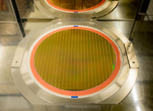
200mm Fabs Add 600,000 Wafers Per Month – Is There an End in Sight?
July 23, 2018
Tracking toward even stronger growth than forecast last year, 200mm fabs
worldwide are gearing up to add more than 600,000 wafers per month from 2017
through 2022, an 11 percent growth rate that will lead to a new high of 6
million wafers per month by the end of 2022, according to the SEMI Industry
Research and Statistics group in its fourth update of the Global 200mm Fab
Outlook report. See chart below.
All told, 56 older and newer facilities will add capacity, with the MEMS, power,
logic and foundry segments contributing the most. To help meet rising demand,
new fabs are under construction. Only six facilities plan to reduce capacity.
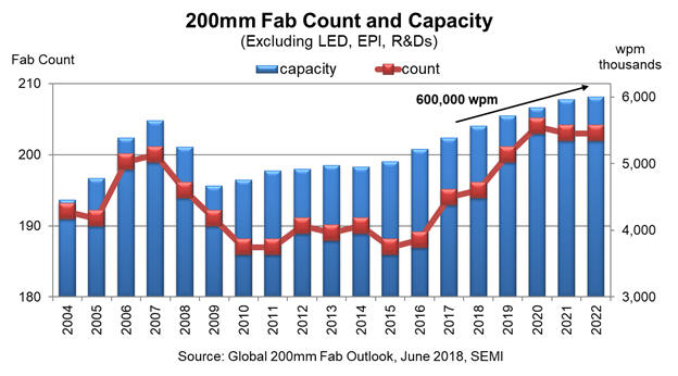
The global 200mm fab count will increase from the 2017 level of the 194 fabs
covered in the report to 203 by 2022. See chart. During the five-year forecast
period, China, at 44 percent, is expected to account for the greatest growth,
followed by Southeast Asia (19 percent), Taiwan (10 percent) and the Americas (8
percent).
However, with strong demand for new 200mm fab equipment, the used 200mm fab equipment market has pretty much dried up. What’s more, the availability of key tools and spare parts has become a primary concern for many device makers.
These headwinds notwithstanding, many companies remain bullish with plans to add
more capacity. The forecast growth of 600,000 wafers per month may ultimately be
a conservative estimate.
SEMI’s Global 200mm Fab Outlook report lists more than 300 facilities and lines
managed by more than 150 companies, providing details on product type,
investment, technology and capacity plans by companies and fabs.
The fourth update of the Global 200mm Fab Outlook report covers data and
predictions from 2011 through the end of 2022, including milestones, detailed
investments by quarter, product types, technology nodes and capacities down to
fab and project level.
The global 200mm fab count will increase from the 2017 level of the 194 fabs
covered in the report to 203 by 2022. See chart. During the five-year forecast
period, China, at 44 percent, is expected to account for the greatest growth,
followed by Southeast Asia (19 percent), Taiwan (10 percent) and the Americas (8
percent).
However, with strong demand for new 200mm fab equipment, the used 200mm fab
equipment market has pretty much dried up. What’s more, the availability of key
tools and spare parts has become a primary concern for many device makers.
These headwinds notwithstanding, many companies remain bullish with plans to add
more capacity. The forecast growth of 600,000 wafers per month may ultimately be
a conservative estimate.
SEMI’s Global 200mm Fab Outlook report lists more than 300 facilities and lines
managed by more than 150 companies, providing details on product type,
investment, technology and capacity plans by companies and fabs.
The fourth update of the Global 200mm Fab Outlook report covers data and
predictions from 2011 through the end of 2022, including milestones, detailed
investments by quarter, product types, technology nodes and capacities down to
fab and project level.
McIlvaine Company
Northfield, IL 60093-2743
Tel:
847-784-0012; Fax:
847-784-0061
E-mail:
editor@mcilvainecompany.com
Web site:
www.mcilvainecompany.com