SEMICONDUCTOR
UPDATE
May 2009
McIlvaine Company
TABLE OF CONTENTS
S. Korea's Hynix to Set up China Chip Processing Unit
AMD Global Foundries and Atic Construct $4.2 Billion Facility
Fab Dreams have Doubters / AMD Still GlobalFoundries' Only Customer
AMD’s Globalfoundries to Ramp with 22 nm Chips
Entegris Speeding up Transfer of Operations
New Company IPDIA Formed to Use NXP’s Fab in France
Vivace Moves Semiconductor Business from Beverly, MA to China
TI Ramps up New Assembly/Test Facility
NEC Electronics, Renesas Merging Chip Units / Spansion & Qimonda Bankrupt
III-V Fabrication Heads to the Middle East in Turkey and Saudi Arabia
Few Unscathed in Worse-than-Thought 2008
South Korean firm Hynix Semiconductor Inc. (KSE:) announced plans to form a Chinese joint venture for handling second-stage memory chip production.
The new company, based in Wuxi, Jiangsu Province, will be owned by Hynix and a local industrial development group. The chipmaker will hold a 45 per cent stake in the joint venture, which will be capitalized at US$150 million.
Hynix will sell equipment from its South Korean and Chinese facilities to the Wuxi Company for roughly US$300 million. By transferring a portion of chip packaging and testing processes to the new firm, it aims to reduce capital investments by more than two trillion won (US$1.6 billion) over five years. The parent will focus on the first stage of chip production and on R&D.
Hynix raised about 700 billion won through a public offering. The move was prompted by the firm's 1.17 trillion won group net loss for the January-March quarter in the face of plunging prices for memory chips.
Hynix Semiconductor Establishes Joint Venture in China
Hynix Semiconductor is to establish a back-end IC packaging joint venture in China with Wuxi Industrial Development Group Company Ltd. Certain equipment currently owned by Hynix in both Korea and China will be purchased Wuxi Industrial Development Group, for approximately US$300 million.
The IC packaging JV will support production at Hynix-Numonyx Semiconductor facility in Wuxi. The new JV reduces the Korean based memory manufacturers’ back-end operations by 20 percent, resulting in Hynix now outsourcing 50 percent of back-end operations.
Advanced Micro Devices (AMD) has begun construction of the $4.2 billion (Dh15.4bn) manufacturing facility of Globalfoundries a joint venture firm formed by AMD and Advanced Technology Investment Company (Atic), which is a part of Abu Dhabi-based Mubadala Development Company.
The Globalfoundries' new facility is coming up in Saratoga County, New York, and expected to be operational by 2011, according to a top official at AMD.
"We closed the deal on Globalfoundries this first quarter and have initiated construction works on Globalfoundries this summer. AMD is expecting to complete the new facility in the next two years. It will manufacture wafers for semiconductor firms globally. As of now, I can't provide any forward looking statement about the new venture," Dirk Meyer, President and Chief Executive of AMD, told Emirates Business.
Mubadala invested about $600 million for 8.1 per cent stake in AMD, which along with Atic announced plans to set up Globalfoundries in October 2008, subsequently the JV became officially operational on March 2 this year. The California-headquartered Globalfoundries has facilities in Dresden, Germany, and New York.
"Globalfoundries is operational as another facility in Dresden is functioning. AMD and Atic have equal shareholding in the Globalfoundries and both the companies can enhance their investment as and when it's required," Meyer said.
AMD has decided to expand its facility in Germany (Fab1) by adding a second 300mm manufacturing unit with bulk silicon capabilities online by late 2009, while the Fab2, the new manufacturing facility of Globalfoundries, is likely to create about 5,000 direct and indirect jobs.
Fab1 with module-1 focuses on production of high-performance 45nm Silicon-on-Insulator (SoI) technology, and with module-2, it's transitioning to 32nm bulk silicon capabilities.
Fab2 will bring in a new state-of-the-art 32nm and smaller features of wafers.
With a capacity to handle 35,000 wafer starts per month, the new facility Fab2 comprises 300,000 sq. ft. Class-100 (ISO Class 5) cleanrooms. The new facility at the Luther Forest Technology Campus, Saratoga County, New York, is coming up over 223 acres.
AMD has received $700m from Atic for a portion of its ownership interests in Globalfoundries, the foundry company assumed responsibility for the repayment of about $1.1bn of associated AMD debt, and Mubadala paid AMD about $125m for 58 million newly issued AMD shares and warrants for 35 million additional shares.
"With the close of this historic transaction, AMD and its committed partners have conceived two strong industry-leading companies capable of charting future courses that will dramatically improve the technology industry," said the chief executive of AMD.
On a fully converted to common shares basis, AMD owns 34.2 percent and ATIC 65.8 per cent in Globalfoundries.
There are still some doubters when it comes to the $4.2 billion computer chip fab being built here at the Luther Forest Technology Campus.
Even though GlobalFoundries Inc. is on the verge of acquiring 222 acres of land at Luther Forest to build the 1.3 million-square-foot factory, some believe the economic boom being touted won't play out. While the company and local business leaders see thousands of new jobs being created regionally, including 1,400 at the plant itself, others are more skeptical.
They includes Adolfo Gutierrez of Brunswick, who has a doctorate in engineering physics from Rensselaer Polytechnic Institute and runs a technology consulting start-up called uBricks Inc.
GlobalFoundries was spun off from Advanced Micro Devices Inc. as a "foundry" to make chips for AMD, and eventually, other companies.
But Gutierrez says that until GlobalFoundries can land business from other chip companies and take it away from powerful Asian foundries such as Taiwan Semiconductor Manufacturing Co. Ltd, he won't be convinced that the Malta project will succeed.
"The land purchase is meaningless, even the start of the construction is superfluous... unless large clients show up very soon," Gutierrez said.
Another doubter is Kyle York of Saratoga Springs, who like Gutierrez has voiced his opinion on various blogs, including those of the Times Union.
York is worried that the battle between AMD and rival Intel Corp. will cause problems for GlobalFoundries. AMD is currently suing Intel in federal court in Delaware over alleged anti-trust allegations, and Intel has threatened to cancel its technology-sharing agreement with AMD. York worries that Intel will scuttle the document; leaving AMD unable to make chips.
"We're left in a dark and silent forest (if that happens)," York said.
York is especially concerned about the cost to the state and Saratoga County, which is building a $67 million water line to Luther Forest so that Fab 2, as the new plant is being called, can use three million gallons of water per day.
New York State’s $1.2 billion incentive package includes $650 million in cash that GlobalFoundries can use for building construction and research and development costs. However, much of the benefits of the package are tax breaks that can only be realized with construction and job creation, and the state can recoup the grant money if certain employment targets are not reached.
Despite the questions that remain, it's all but certain now that GlobalFoundries will be moving forward very soon with about $800 million in contracts to build Fab 2. (GlobalFoundries other manufacturing facilities, known as Fab 1, are located in Dresden, Germany).
Any day now, GlobalFoundries expects to close on the purchase of the Luther Forest land for an estimated price tag between $7 million and $8 million. At the same time, the company is expected to name M+W Zander the general contractor for the project, and the first contract for site clearing will be awarded.
An official groundbreaking could take place by July, and construction of the building "shell" is expected to continue through 2010. Full scale production is slated for 2012, after the wafer manufacturing "tools" are installed and qualified.
It's expected that construction will create 1,600 jobs for laborers and project managers, with an annual payroll of $106 million.
That is why the Chamber of Southern Saratoga County held a half-day summit Wednesday for school guidance counselors and administrators at Ballston Spa High School about opportunities in the construction industry with high tech projects.
"All of a sudden, people have started to realize this is what our future's going to look like," said Peter Aust, the chamber's president. "One of the first sectors is going to be construction. It's going to be a building boom for the next 15 to 20 years."
One of those speaking at the event in Ballston Spa was Alan Asadoorian, director of construction for M+W Zander's U.S. operations. In addition to being the likely general contractor for the Fab 2 project, M+W Zander also built the Albany NanoTech complex and has been involved with projects for IBM Corp. and other chip companies.
Asadoorian said he plans to grow the local project staff from between 35 and 50 people to as many as 125 in the next several years. The company has an office at the Watervliet Arsenal.
"We're prepared to start the construction," Asadoorian said. "We'll be hiring contractors and subcontractors over the next several years."
Two weeks ago, GlobalFoundries invited analysts and technology journalists from around the world to its offices in Malta to look at the Luther Forest site and learn about its plans to make chips for AMD and others.
Those contacted by the Times Union after they returned home said they were hopeful that GlobalFoundries would build Fab 2 and be successful. They also said that it's possible that GlobalFoundries would build additional factories, known as modules, on the site.
"I have no doubt that Fab 2 will get built," said Jim McGregor, chief technology strategist with In-Stat, a research and consulting firm in Scottsdale, Ariz. "GlobalFoundries has an advantage of some very deep pockets right now. The later fabs will depend on the market and the company's ability to land some key customers, but right now they are in a great position."
Those deep pockets belong to Advanced Technology Investment Co., which is owned by the oil-rich Emirate of Abu Dhabi. ATIC, which owns GlobalFoundries in a joint venture with AMD, invested $2.1 billion in the spinoff and has promised to invest between $3.6 billion and $6 billion in the company over the next five years to expand manufacturing.
Scott Bicheno, editor of a British online technology publication called Hexus.channel, said that it is difficult to predict whether GlobalFoundries will be a success even before it builds Fab 2.
However, he said there "does seem to be a fair bit of momentum behind" the project and if GlobalFoundries can get more customers beyond AMD, it should do well.
"If it does that there's no obvious reason why it shouldn't be a success and, in theory, grow enough to build the other two modules it has the space for," Bicheno said.
Malta Town Supervisor Paul Sausville said last week he sees fewer and fewer doubters as the Fab 2 project progresses.
"There are always a few people," Sausville said. "Some people are joking just for fun. I think it's going to happen. Construction activity is going to be very intense."
Globalfoundries, the spun-off manufacturing arm of AMD, provided a first glimpse at the plans of its 1.3 million square foot chip factory to be built at Luther Forest Technology Park in Saratoga County. The construction of the plant is still on schedule, but it will be more expensive than originally planned and technologically much more advanced: The factory will start production at 32 nm and the half-node 28 nm, but ramp quickly in 22 nm.
It has been almost three years since AMD unveiled its plans to build a chip factory to support its expansion. Back then, in June of 2006, AMD was flying high with its Opteron and Athlon X2 processors that took over market share from Intel almost at will. AMD’s market share gains were limited by its production capacity, especially with new customers such as Dell, and an expansion plan made sense. However, AMD underestimated Intel’s strength and ended up in huge debt, supported by the $5.4 billion acquisition of ATI, and some believe that the company remained only alive because Intel needs AMD to stay out of more antitrust trouble.
Globalfoundries is the result of AMD’s troubles, and has been created through $6 billion in committed investments from Abu Dhabi-based Advanced Technology Investment Company (ATIC), which holds 65.8 percent of the company. AMD holds the remaining 34.2 percent of the contract manufacturer. Globalfoundries currently has AMD as its sole customer, and runs its production in its Dresden, Germany-based fabs, now called Fab 1 Module 1 and Module 2 (formerly AMD Fab 30 and 36). Fab 2 will be built in the Luther Forest Technology Park, just outside Saratoga Springs, NY, on 223 acres of land.
The original plans outlined a 1.2 million square foot building that would produce 32 nm processors and cost about $3.2 billion. Since 2006, those estimates have changed a bit – the building, which will begin construction this summer, will have more than 1.3 million square feet and cost about $4.5 billion, including land acquisition and production equipment. The fab will be larger than Intel’s largest fab, located in Kiryat Gat, Israel, and will have more floor space than the Chrysler building in New York City (1.2 million square feet). Globalfoundries said that it will take about 5 million man hours to build the first module of the fab. The fab itself will have about 883,000 square feet, while the cleanroom will measure about 300,000 square feet. AMD said that, at full production, the facility will be able to crank out about 35,000 wafers per month, which is more than the Dresden fabs, which have a capacity of 25,000 wafer starts each. Intel’s fabs are rumored to have a capacity of about 30,000 to 35,000 wafer starts per month each.
Globalfoundries recently showed the area of the future campus to journalists. There isn’t much to see yet, with the exception of streets and bike paths that were built as a contribution by the local government. Touring the Luther Forest Technology Park still requires a capable SUV in some areas. Globalfoundries has rented space in an office building within the Park, which will have space for about 35 employees for now. We were told that former AMD CEO and chairman and now Globalfoundries Chairman Hector Ruiz is present at the campus quite a bit, while the new investors from ATIC have remained in the (public) background so far.
What makes this new fab interesting is the fact that it is likely to be among the most advanced chip factory when it goes into full production 2012. Globalfoundries will be accepting 32 nm and 28 nm designs initially and ramp in 22 nm in 2012. If that plan will turn into reality, the manufacturer will be able to close the gap to Intel from today’s 12-18 months to a time frame that is closer to 6-9 months. And that achievement will be critical for the company to attract customers that compete with Intel. As the construction of new fabs will get more expensive (already today, only Intel and Samsung are the only semiconductor developers that are able to build working financial models around new chip plants) chip designers need to keep up with Intel and it would be a major advantage for Globalfoundries to stay close to its former rival, which now, at least in theory, could be a future customer. Globalfoundries said that it taped out first 32 nm SRAM silicon in Q4 2008 and will begin producing high-k metal gate chips in the first half of next year.
An interesting side note is the fact that the factory is located close to the University of Albany’s College of Nanoscale Science and Engineering (CNSE), which is considered the top school for chip development manufacturing in the United States. The school is trying to attract all the big names in chip manufacturing to research manufacturing techniques in the schools clean room facilities – right next to each other. And it appears that the idea is working very well, as the presence of companies such as IBM and Intel is business incentive enough for other companies to rent clean room space from the university.
There are massive investments taking place that other companies and students can take advantage of, such as Extreme Ultra Violet (EUV) chip printing systems – an immensely expensive technology that is now expected to become a reality at the 15 nm node. The school currently trains 160 grad students, who, by the way, do not pay for the education. The school pays a salary of about $25,000 per year and assumes the additional per-student cost of about $75,000 per year). It is a fascinating place to visit and if you are interested in seeing a chip factory from the inside, you should contact the CNSE staff, who gladly shows the facility especially to school classes.
For Globalfoundries, of course, the proximity to the CNSE is an advantage to enter partnerships to develop manufacturing techniques and recruit knowledgeable staff for its fabs close by.
There is no lack of excitement for the future of the new company. And will certainly be interesting to see how the company will develop and which customers it can attract.
Entegris Inc aims to make its Kulim Hi-Tech Park (KHTP) facility the group’s largest manufacturing center by the year-end.
Group chief operating officer Betrand Loy said to achieve this, the group was now accelerating the transfer of its manufacturing and non-manufacturing activities for semiconductor protective material products to the facility.
“We plan to spend between RM40mil and RM50mil to upgrade the KHTP plant over the next two years. To date, Entegris has invested about RM210mil in the facility.
Bertrand Loy ... ‘We plan to spend RM40mil to RM50mil to upgrade the KHTP plant’
“We will also raise the headcount at the KHTP facility to 750, from the present 488, in 2010 when the semiconductor industry is expected to recover,” he told StarBiz.
About 15 percent of the new staff to be hired in 2010 would be engineers and technical personnel, he added.
Loy said that by the year-end, the KHTP plant would accommodate some 30 percent of the group’s staff of 2,300 worldwide.“This year, we plan to bring over manufacturing and support activities for six to seven new products to KHTP,” he added. These products include a new range of gas filters and purifiers, wafer process carriers and micro-environment and reticle pods used to control contamination in the manufacturing processes of the semiconductor industry.
“We expect the utilization of wafer fabrication capacity in the global semiconductor industry to reach 80 percent to 90 percent in early 2010,” he said.
Loy said the first quarter saw a 70 percent drop in global semiconductor business compared with the same period a year earlier.“The semiconductor sector reached its peak in the second quarter of 2008. We expect business to pick up in the second and third quarter of this year,” he said.
Loy said Entegris was slowly shrinking its operations in the United States and shifting them to Kulim. Entegris now has manufacturing and service centers in Massachusetts, Minnesota, Texas, and Colorado, as well as in France, Japan, South Korea, Singapore and Taiwan.
“At present, the group’s research and development (R&D) work is done in the United States and Japan, with some design and development works for products supporting data storage already established in KHTP. “But we want to transfer a fair share of such activities to Malaysia, so that the R&D work can be close to the manufacturing activities in KHTP,” he said.
Loy said the transfer of the R&D capability was to reduce time on product development and to respond faster to customers’ needs.
“Currently, more than 50 percent of our sales come from Japan and (other parts of) Asia. Some 9 percent of the group’s revenue will be spent on R&D this year,” he added.
To train the necessary skilled workers for the KHTP facility, Entegris has taken part in the Northern Corridor Industrial Technical Enhancement Scheme.
Entegris (Kulim) plant manager Chai Eng Leng said that under the program, the company had taken in 10 fresh graduates since last year for training at the KHTP facility.
“These graduates will undergo a one-year internship with Entegris. After that, we will decide whether to hire them, based on their performance. We will take in 15 more fresh graduates this year,” he said.
A new company, named IPDIA, has been created with support from the French Ministry of Economy, Industry & Labor and local authorities as well as over €5 million from NXP, Prime Technology Ventures, Emertec Gestion, Masseran Gestion NCI Gestion and CEA Investissement. IPDIA will use NXP’s Cote de Nacre facility, near Caen in Northwest France to fabricate unique 3D silicon devices.
“The technology developed in Caen has great potential and can be used in multiple end-markets, noted Jelto Kromwijk Smits, partner at Prime Technology Ventures. “IPDIA has acquired a unique passive integration technology, and we are very excited to be in the position to support the company in the coming years on its growth path.”
IPDIA is to initially employ 90 people, the majority of whom will be recruited among NXP’s laid-off employees from the facility.
Franck Murray, one of the founding directors, becomes CEO of IPDIA. Murray has more than 25 years of experience working in the semiconductor industry.
In the highly competitive semiconductor industry, setting up an office in China is nothing new — many of the manufacturing facilities and potential customers are located there. But to move an entire company 6,700 miles away is something different.
Nonetheless, that is the path taken by Vivace Semiconductor Inc. and its CEO, Cary Ussery.
Originally founded in Beverly in 2006, the maker of multimedia processors began a slow migration to China with its 2007 acquisition of Beijing-based component maker General Circuits Ltd. Shortly thereafter, Ussery moved to China full time, and since then Vivace’s employee base of 70 people has become more Asia-centric. Vivace still has about 15 engineers working in Rochester, N.Y., but its operations, management, and even servers are now located in Beijing.
Ussery cites several reasons for the move, though none related to the cost of labor. He still believes the bulk of chip design expertise lies in North America, but the expertise in analog circuits and the components that go along with Vivace’s chips are in China.
“It wasn’t about driving down engineering costs,” he said. “But as a semiconductor company today, you can’t just provide a chip. You need to provide a system that can be used out of the box, and a lot of that expertise is here (in China).”
Ussery also points to funding and support from the local and national Chinese governments that helped Vivace set up shop. He declined to say how much funding the company has received, but said, as an example, that it is in line for a new funding program that could bring the company $5 million to $10 million this year to help bring its products to market.
“Economic stimulus here doesn’t go into savings banks, but goes into helping specific industries,” he said. “There is really a drive to have companies grow here.”
Vivace has raised $10 million in venture capital and is backed by three Asian VC firms — Dragonvest Partners of Shanghai, Hotung Capital Management of Taiwan and China Renaissance Capital Investment of Hong Kong. However, the firm’s lead investor is Waltham’s Kodiak Venture Partners, and Kodiak founder and general partner Dave Furneaux sits on Vivace’s board.
The scenario, said Furneaux, makes management of his portfolio company challenging, but it was a move Vivace had to make.
“Venture capital is a local business, and it is a unique situation for us to be invested so far away,” he said. “Vivace simply needed to be in China given what they do and who they sell to.”
Ussery hasn’t completely abandoned his country of birth. He maintains that the design expertise remains higher in the U.S., and once Vivace begins generating revenue — its first product went to market last fall and the next generation is due at the end of this year — he may begin to build out his work force on U.S. shores.
Texas Instruments' newest assembly/test facility expands its overall capacity in the Philippines, focusing on WCSP and QFN packaging. The Clark facility is following a relatively recent industry trend -- it's on track to achieve Leadership in Energy and Environmental Design (LEED) certification this year.
Nearly two years ago, Texas Instruments Inc. (TI, Dallas) announced plans to build an assembly/test facility within the Clark Freeport Zone in the Philippines — with the goal of becoming one of the most environmentally efficient sites in the world. The Clark facility, as it’s known, is now up and ramping, focusing on the latest wafer-level chip-scale packaging (WCSP) technologies that eliminate conventional packaging steps like die bonding, wire bonding, and die-level flip-chip attach processes.
Quad flat no-lead (QFN) packaging is also receiving attention from TI, with capacity being added to qualify QFN packages at Clark. QFN packages are desirable primarily for their electrical and thermal performance, but can also provide a cost reduction.
Why the Philippines? TI is no newcomer to the Southeast Asian republic. Baguoi City is home to one of its most sophisticated assembly/test sites, which has been operating since 1979. The Clark facility is situated a short distance away, and adds nearly 80,000 m2 (860,800 sq. ft.) of capacity in the Philippines for the chipmaker.
TI’s overall high-level packaging strategy is still about addressing customer needs, said Mahadeven Iyer, director of TI’s worldwide semiconductor packaging business. “We have the expertise and the flexibility attached to the internal and external manufacturing options. The three key factors that we look at in our overall packaging strategy are cost, performance and form factor,” he said. “TI provides a core competency and expertise in chip/package codesign, materials characterization, process development, assembly process development, and reliability. In terms of flexibility, we have internal packaging development and manufacturing, as well as enjoy strong partnerships with subcons.”
Iyer considers packaging an integral part of the chip and overall system, as well as a key differentiator to meet customers’ needs. “Packaging technology is more of a system solution than a single-chip solution, addressing system drivers such as shorter product lifecycles and multifunction integration,” he said.
Iyer said he is seeing a trend emerge toward thermal modeling and analysis, key areas in which the industry now has the right tools and capabilities. Thermo-mechanical design is equally important when addressing complex substrates, warpage issues, and thermo-mechanical modeling. “Modeling tools are becoming very handy for fine-pitch flip-chips with complex substrates — including solder bump flip-chip applications as well,” Iyer said. “From a materials point of view, developers and suppliers are working with TI on some challenges with flip-chip package materials. As we look ahead, there is potential for nanomaterials to enhance performance. As for the assembly process, there are opportunities for fine-pitch flip-chip assembly, copper wire bonding, WCSP and 3-D integration.”
Design tools are a technology challenge right now, according to Iyer. As packages become more complex, codesign is becoming much more prominent. “Tools need to be synchronized with the chip design tools,” he explained. “Chip design tools have been around longer than the packaging tools; they’re more mature. There’s a gap that needs to be filled as we look at package design for more complex packaging on flip-chip, wafer-scale and 3-D packaging.”
From a pure materials assembly process point of view, integration challenges will require advanced materials, and processes need to be developed, Iyer noted. “That’s where TI is positioning itself in terms of having WCSP, 3-D integration and fine-pitch flip-chip options,” he said.
Substrates are another area Iyer mentioned as being a key packaging technology challenge — one which he expects will be around for the next five to 10 years.
The Clark facility is following a relatively recent industry trend — it’s on track to achieve Leadership in Energy and Environmental Design (LEED) certification this year, which TI’s Baguoi facility has already accomplished. LEED is a voluntary standard for developing high-performance, sustainable buildings that take a holistic approach to design and sustainability by improving water-use efficiency, materials and resources, as well as focusing on indoor environmental quality. TI’s facilities in the region make up one of the largest LEED-certified assembly/test sites in the world.
NEC Electronics Corp. and Renesas Technology Corp. said they have agreed to merge their operations and form the world's third-largest semiconductor maker.
The companies aim to finalize negotiations in July and combine their businesses from April of next year, they said in a joint press release. Reports of a merger had been circulating for weeks.
NEC Electronics, majority-owned by electronics giant NEC Corp., and Renesas said they are facing increasing competition in the chip industry, and market conditions have deteriorated since the global economy ground to a halt.
The semiconductor business requires massive upfront investment for production equipment, and selling prices face constant downward pressure as technology advances. A merger would allow the two companies to phase out older, less productive lines and better leverage economies of scale.
Other chip companies are also struggling. U.S.-based flash memory maker Spansion Inc. and its subsidiaries filed for bankruptcy in March, and German manufacturer Qimonda AG declared bankruptcy in January.
NEC Electronics's stock was up 5.4 percent to 1,080 yen, while the benchmark Nikkei 225 stock average inched up 0.2 percent. Renesas is jointly owned by Hitachi Ltd. and Mitsubishi Electric.
New Saudi and Turkish institutions are gearing up with high-end kit, including MOCVD systems, for III-V device development and processing.
Compound semiconductor research looks set to receive a boost in the unlikely Middle Eastern locations of Saudi Arabia and Turkey.
The King Abdullah University of Science and Technology (KAUST), located in Jeddah and backed to the tune of $10 billion by the Arab state's leading crude oil producer Aramco, is investing heavily in semiconductor equipment.
KAUST is still under construction, and due to open in time for the new academic year on September 5, 2009.
Meanwhile, cleanrooms at Turkey's $120 million Institute of Materials Science and Nanotechnology (UNAM), located at Bilkent University in Ankara, are scheduled to be “fully functional” by June.
Tony Eastham, director of laboratories at KAUST, told compoundsemiconductor.net that among the many areas of cutting-edge research under investigation at the new institution's Advanced NanoFabrication Center will be “nanoelectronics, photonics, LEDs and functional materials”.
“We are establishing leading-edge facilities,” Eastham added.
Already set up with Class 1000 (ISO Class 6) and Class 100 (ISO Class 5) cleanroom capability, and instrumentation including nanoimprint lithography and an electron-beam writer, KAUST last week ordered more high-end equipment from Oxford Instruments Plasma Technology (OIPT).
OIPT says that the order comprised “multiple plasma etch, deposition & growth systems”, including several reactive-ion-etch PlasmaLab systems, PECVD equipment, and a FlexAL tool for atomic layer deposition (ALD).
Eastham confirmed with laboratory manager Xixiang Zhang that MOCVD equipment is also set to be installed, although there are no current plans to purchase an MBE system.
At UNAM in Turkey, researcher Necmi Biyikli confirmed that two inductively coupled plasma (ICP) etch tools from Surface Technology Systems (STS) were on order.
Biyikli told compoundsemiconductor.net that one of the tools would use chlorine-based process gases to etch III-V materials, with the second using fluorine for work on silicon.
“Combining the STS tools with other deposition/etching systems, as well as e-beam lithography, nano-imprint lithography and focused ion beam systems, we will have the ability to fabricate novel, proof-of-concept nano-scale devices,” Biyikli added.
UNAM's 400 m2 (4,304 sq. ft.) cleanroom is part of the first such national user facility for III-V work in Turkey.
Users will have access to a range of epitaxy equipment, including MOCVD, MBE and low-pressure CVD tools, as well as the latest STS kit, which Biyikli says will be one of the “workhorses” of the UNAM cleanroom.
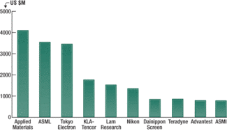
A month ago Gartner pegged preliminary 2008 capex at a -25 percent slide to ~$33.46B. Turns out the firm was about $3B on the high side — its final tally pegs 2008 semiconductor capex at just $30.7B, down -31.7 percent from 2007.
With the combined impact of memory oversupplies and then a demand crash across the entire industry, 2008 will go down as “one of the worst years in the history of the semiconductor capital equipment industry,” noted Klaus Rinnen, managing VP for Gartner’s semiconductor manufacturing research group, in a statement.
There was little change among the top 6 firms, though growth declines varied as some tool types and suppliers did notably better than others. Lithography segments, for instance, rode demand for 193nm DUV immersion steppers, sinking -25 percent (-29 percent for track tools), better than the industry average; ASML leapfrogged TEL as the No.2 company in Gartner’s rankings thanks to this trend.
Top 10 worldwide semiconductor manufacturing equipment vendors (US $M). Data includes revenue from acquisitions in 2008 for the entire year; 2007 data is before acquisitions. Growth is organic as well as through acquisitions. (Source: Gartner)
In backend segments, packaging/assembly sunk -24.5 percent, with more traditional die-level packaging taking the brunt of it (-30 percent+ Y/Y for interconnect and die bonder sales), while advanced packaging lithography and wafer-level packaging tools “eked out growth.” SoC test and RF test “remained strong” in the automated test sector, which overall gave back more than 31 percent; not surprisingly memory test demand plunged -60 percent. (VLSI in its year-end rankings had noted Teradyne’s performance was largely due to its early-year acquisition of NexTest.)
WORLDWIDE HIGHLIGHTS
Global shipments of polysilicon surged 41 percent from the start of 2008 to year’s end, thanks to new capacity coming online—and even the late-year meltdown across the semiconductor industry and beyond didn’t curtail growth, according to data from SEMI.
Global PV output surged to 5.5GW in 2008 according to preliminary data from the European Photovoltaic Industry Association (EPIA). Meanwhile, the US-based Solar Energy Industries Association said domestic PV manufacturing capacity increased 65 percent vs. 2007, and production rose 53 percent.
Applied Materials and DISCO plan to develop wafer thinning processes for fabricating through-silicon vias (TSV) for 3D chips, using Applied’s etch/dielectric deposition/PVD/CMP systems and DISCO’s grinding tools.
FlipChip International and SMIC have agreed to align their technology and product roadmaps for 300mm bumping solutions at a number of technology nodes.
As planned, Axcelis Technologies has closed the sale of its 50 percent interest in Japanese JV SEN to partner Sumitomo Heavy Industries, with a chunk of the $122.3M in proceeds used to pay off overdue notes obligations.
USA
The Semiconductor Test Consortium has dissolved and transferred its infrastructure and Semiconductor Test Interface eXtensions (STIX) working group to SEMI’s new special interest group, the Collaborative Alliance for Semiconductor Test (CAST). The STC’s OPENSTAR trademark and logo will be transferred to Advantest.
Qimonda’s 300mm/65nm-capable, 38,000 wafer starts/month fab in Richmond, VA is officially up for sale; if a buyer is not found, a tool sale will quickly follow.
Rubicon says it has grown the world’s largest sapphire crystal—a 200kg (441lb) “super boule,” more than twice the company’s previous efforts—from which it can make optical components and wafers larger than 300mm.
WRS Materials has acquired Isonics Semiconductor Group, adding 90nm particle-grade reclaimed wafers and expanded 200mm-300mm production, and has secured $9.9M in funding.
3D IC packaging startup Imbera has secured $15M in Series B funding, which will be used to bring online a high-volume manufacturing operation in Korea and support R&D activities in Finland
Portland, Oregon reportedly is a finalist for a new $1.1B investment from Siltronic and an unnamed European investor to build a new factory, according to a local paper citing “an internal city e-mail.”
SUNY/Albany’s College of Nanoscale Science and Engineering (CNSE) has opened a new $150M NanoFab East center, part of a $1B package from IBM and partners of which the bulk will go toward 22nm-node development.
ON Semiconductor has licensed 110nm technology from LSI Logic for a new ASIC platform, to be produced in its wafer fab in Gresham, OR.
ESI and Zygo have called off their merger proposed in Oct. 2008; as a result Zygo will pay $5.4M in breakup fees, and an additional $1.2M if it finds another buyer within six months.
Akrion Systems has appointed COO Michael Ioannou as president of the company, replacing Jim Molinaro who left to pursue other interests.
ASIA FOCUS
It’s official: Taiwan Memory will partner with Japan’s Elpida for DRAM technology. But despite buzz about finding room for everyone in Taiwan’s proposed DRAM restructuring, Micron CEO Steve Appleton says “the deal that’s OK with Elpida is not OK with us,” so it’s seeking to raise $450M from selling stocks and notes.
Japan says it will end a three-year old punitive import duty on Hynix chips later this month after determining the company no longer benefits from state or federal government aid.
Toshiba reportedly is considering procuring solar panels from Sharp and other suppliers to strengthen its push into the PV sector.
Nippon Steel is nearly ready to ramp output and sales of single- crystal silicon carbide (SiC) wafers, the first Japanese company to reach full production of the technology.
Despite rumors of “large-scale business redeployment,” Intel’s Dalian plant is still on schedule, according to a GM cited by a local paper; construction of six main buildings is almost complete, and a data center will be online within days.
Local reports suggest China is working on a plan to establish a “union” in its silicon materials industry to help cope with the ongoing financial crisis.
Hitachi and Mitsubishi Electric are injecting $571M into their Renesas JV via a new shares issuance.
Elpida has acquired a portion of ownership from Taiwan’s Powerchip Semiconductor in their DRAM JV, Rexchip, enough to make it a 52 percent owner and thus convert the JV to a consolidated subsidiary.
ENN Solar Energy Co. Ltd. has produced China’s first 5.7m2(61.33 sq. ft.) tandem junction thin-film photovoltaic solar panels on an Applied Materials SunFab line.
EURO FOCUS
The European Patent Office has revoked a patent from the U. of Neuchatel’s regarding amorphous silicon PV technology, which had been licensed to Oerlikon—and was the crux of a suit against Sunfilm, which uses Applied Materials’ SunFab tools.
CEA/Leti and IBM have signed a five-year deal to pursue development of materials and processes for 22nm CMOS and beyond.
Applied Materials has signed a five-year contract to support its wafer processing systems at Tower Semiconductor’s Fab 2 200mm manufacturing facility in Israel, “at a low, predictable cost.”
EV Group and CEA/Leti have formed a joint development program to use EVG’s 300mm temporary bonding and debonding technology for work on TSVs and 3D integration.
Soitec says its “Smart Stacking” circuit stacking capability, which transfers thin layers of processed wafers onto a variety of materials, is ready for manufacturing and licensing.
Despite Freescale’s choice to shutter its operation in East Kilbride, Scotland, National Semiconductor says closures in its other sites means more work will be coming to its facility in Greenock.
The Linde Group says it has a new long-term contract to supply gases for next-generation thin-film PV module production at Masdar’s manufacturing site in Erfurt, Germany.
Merck says it will sponsor work on semiconductor nanoparticles from Israeli startup QLight Nanotech for use in display applications.
Under a new pact, Infineon will supply components and a technology license to Robert Bosch for low-voltage power transistors.
Weeks after ASMI agreed to drop swords with key investor Hermes, hedge fund Centaurus Capital has lowered its ASMI stake to <5 percent, down from 7.22 percent. Two new board members also have been nominated, one to replace Leon van den Boom who resigned citing “diverging views” with the company’s direction.
ARISE Technologies says its Line 2 in Bischofswerda, Germany has produced its first monocrystalline PV cells on schedule, with an efficiency range of ~15 percent-16 percent.
McIlvaine Company,
Northfield, IL 60093-2743
Tel: 847-784-0012; Fax: 847-784-0061;
E-mail: editor@mcilvainecompany.com;
Web site: www.mcilvainecompany.com