OTHER ELECTRONICS & NANOTECHNOLOGY
UPDATE
May 2010
McIlvaine Company
TABLE OF CONTENTS
Jamia Gets Grant for Nanotechnology Research
Dow Chemical to Open Korean Research Center
Dupont to Buy Minority Stake in Chinese Chemical Maker
Victron Plans Opening in Mexico
Bar Ilan Institute of Nanotechnology and Advanced Materials
Plans for Princeton's Andlinger Center for Energy and the Environment Completed
IBM and Lithuania Plan Research Centre in Lithuania
Emerson Opens $30 Million Global Innovation Center
JC-Saft Battery Plant Construction on Schedule
NC's Core Technology Expands for Medical Customers
NanoString Gets ISO Certification
LHU Unveils Plans for New Science Center
Russia to Launch Two Nanotechnology Plants
Intel to invest Rs.817 crore in Mexican Design Centre
Educational Facility in Malta Opens
Bayer MaterialScience Opens Carbon Nanotube Facility
Albany’s Nanotech Complex Creates Jobs in New York State
Nokia Siemens Builds TD-LTE Open Lab in Hangzhou
Victron Expands to Rosarito, Mexico
Agilent Launches "Green" Campus in India
Show Me the (NANO) Money - A decade of U.S. Federal Investments in Nanotechnology
The Jamia Milia Islamia will carry out advanced research in nanotechnology, the only university in India to do so, a university statement said. Given the growing applications of nanotechnology, the varsity has been given Rs.8 crore (Rs.80 million) government funding for carrying out two projects in the field.
The 91-year-old Jamia, which runs over 200 courses, will not only be the first university to carry out research in “Synthesising Single Wall Carbon Nanotubes” but also the only institution in the country to carry out research in nanotechnology, said the statement.
The funds sanctioned by the Department of Information Technology will be used by the varsity’s physics department and applied sciences department. The varsity runs an M.Tech program in nanotechnology.
The university has been doing cutting edge research in the areas of nanoscience and nanotechnology and in recognition of that it has already been awarded a project on Carbon Nanotubes by the Defense Research and Development Organization (DRDO), the university said.
The Dow Chemical Co. said its electronic materials subsidiary will open a new research and development center in Seoul next year. In the last 10 years, Dow Electronic Materials has invested more than $300 million in the Korean electronic materials market. The new center will focus on advancing flat panel display technologies, semiconductor devices and related applications. The new facility will employ more than 200 scientists and engineers. The multistory complex will feature cleanroom capability, chemistry and application laboratories and office space.
DuPont plans to buy a minority stake in a Chinese chemical maker for an undisclosed sum. DuPont said the deal to buy Changshu 3F Zhonghao New Chemical Materials Co., is subject to final agreements and Chinese government approval. The acquisition will expand DuPont's reach into the fluorochemical market. Fluorochemicals are used in cooling, electronics and personal care products.
Victron, Inc., a premier electronics manufacturing services (EMS) supplier of end-to-end manufacturing solutions to Fortune 500 companies, will host a grand opening celebration at its Rosarito, Mexico facility on June 3, 2010. Customers, suppliers, and local and state representatives will be on hand for the ribbon cutting ceremony and event.
Milla Woo, Vice President of Global Sales and Marketing, said, "This new site represents a significant step in Victron's global expansion strategy. We have equipped this facility with a copy exact approach to our manufacturing process and standards of quality that will enhance our leadership position in the EMS industry and bring alternative business solutions for our customers."
Victron's 30,000 sq. ft. Rosarito facility offers printed circuit board assembly, in-circuit testing, functional testing, subsystem and final system integration for its OEM customers in the medical and industrial segments as well as other markets. With a close proximity to the San Diego border, Rosarito offers a quiet community with a highly experienced local workforce.
Victron has manufacturing sites in Fremont, CA and Rosarito, Mexico, providing end-to-end manufacturing solutions from design services through complex product manufacturing of full system integration, product fulfillment and logistics for leading OEMs. Victron offers highly flexible, scalable, and fast response manufacturing and supply chain services using proprietary software tools, execution-oriented manufacturing processes and technical expertise.
Bar Ilan Institute of Nanotechnology and Advanced Materials
Research efforts are concentrated within six core areas that were identified when the Bar-Ilan Institute of Nanotechnology & Advanced Materials was established. Each research area has its own dedicated Center within the Institute. The six centers of excellence are: Nano-Materials Center, Nano-Medicine Center, The Dahan Nano-Energy Center, Nano-Magnetism Center, Nano-Cleantech Center and Nano-Photonics Center.
The Nano-Materials Center
The field of nano-materials is the very foundation of nanotechnology and nanoscience. The search for innovative synthesis methods and ways to prepare nano-scale materials in various forms, such as particles, rods, and nano-layers, is the very first stage in any nanoscience application. The BINA Nano-Materials Center is at the forefront of this seminal work – researching new methods and approaches to synthesize and characterize size, structure and chemical composition of materials and overcoming the formidable challenges involved in controlling the preparation of nanoscale materials to ensure they possess the desired properties to advance applicative research.
A group of leading Bar-Ilan University scientists has been working on nano-scale materials since the mid-1990s. The breadth and scope of this work resulted in Bar-Ilan University being ranked 3rd in the number of citations for advanced materials publications between 1999 and 2004. Since then, the Nano-Materials Center has expanded its ranks and influence, and today is home to no less than 17 research groups. Among the many groundbreaking projects these groups are working on are Prof. Aharon Gedanken’s research to develop new and innovative methods for the preparation and synthesis of nano-scale materials. Prof. Chaim Sukenik, the Nano-Material Center’s Director and a world-renown pioneer in this field, leads a group working on self-assembly of nanoscale layers with a variety of highly important properties, such as non-flammable monolayer covers. Prof. Shlomo Margel and Prof. Jean Paul- Lellouche are applying methods to synthesize functional materials for medical applications that will bring about important paradigm shifts in the world of drug delivery and diagnostic medical imaging. Other areas of interest include the study of chiral surfaces and monomolecular films on liquid surfaces. These, and scores of other projects, are setting the pace of advanced materials research not only within the field of nano-materials, but throughout the entire spectrum of nanotechnology research.
The Nano-Medicine Center
One of the most exiting areas of nanotechnology, and that holds so much promise for improving the lives and health of millions, is nano-medicine. At the Bar-Ilan Institute of Nanotechnology & Advanced Materials, this work is spearheaded by Professor Uri Nir, Director of the Nano-Medicine Center and Vice Dean of the Faculty of Life Sciences.
Current research in the Center focuses on one of the greatest challenges of modern medicine: developing new and innovative approaches to treating cancer that address the disease at the very core of its deadly mechanisms. For example, Prof. Nir’s work has revealed a “smoking gun” – an enzyme that in several tissue types plays a pivotal role in the onset of cancer and has shown the ability to directly strike down or halt the mechanism common to the disease process in prostrate, breast and colon cancers. Other members of the Nano-Medicine Center are researching new mechanisms, innovative chemotherapeutic drugs and targeted drug delivery methods to site-specific cells in the area of oncologic diagnostics and treatment as well. A veritable interdisciplinary rainbow of chemists, biologists and physicists in the BINA Nano-Medicine Center collaborate closely to advance the development of targeted delivery of anti-cancer drugs inside living cells. Examples include Dr. Yoav Paas’ significant strides in anti-cancer drug delivery through ion channels in cell membranes and Prof. Benny Ehrenberg’s discoveries using fluorescent light treatment to prevent disease. Nanotechnology is being applied in the realm of diagnostics as well, with projects related to magnetic nanoparticles that can be imaged using MRI techniques.
The Aharon & Rachel Dahan Nano-Energy Center
Research for sustainable energy sources is one of the highest priorities in supplying global energy needs due to the volatile state of the world’s oil supplies and markets. In response to growing demand for energy and the need to drastically reduce carbon dioxide emission, scientists across the globe are joined in the quest for renewable, carbon free, clean energy sources.
Leveraging the inherent interdisciplinary approach of nanoscience, Bar-Ilan University researchers are playing a vital role in developing renewable energy applications, specifically in the fields of photovoltaics, energy storage, solar thermal energy, energy conservation, and basic research.
Prof. Doron Aurbach is world-renown for his work in the field of energy storage and conversion. Based on the premise that battery materials composed of nano-scale particles can provide a higher current extraction rate, his team is making serious progress in applying new materials for rechargeable batteries and super capacitors. Other examples of the working being conducted in the Center include the research being carried out by Prof. Arie Zaban, the Director of BINA and the Nano-Energy Center, in the field of dye-sensitive solar cells that are expected to be more cost-effective than current silicon-based solar cells. In addition, Prof. Zaban’s group is applying new research in nano-materials to develop energy-related components, such as innovative air electrodes for fuel cells based on a nano-structure catalyst. Using nano-scale thin superconducting films for studying magnetic flux dynamics, Prof. Yosef Yeshurun’s original work in the field of superconductivity is a vital link in this exciting area. Dr. Joseph Frey has introduced an innovative approach to build a bulk heterojunction, based on self-assembled p-conjugated rod-coil block copolymers, converting them into functional organic/inorganic nano-composites, such as titania/conjugated polymer and conjugated polymer/carbon nanotubes. These new nano materials are expected to enhance charge separation and thus improve the efficiency of the photovoltaic cells. Prof. Moshe Deutsch is studying the electrode-electrolyte interfaces produced by ionic liquids as promising electrolytes for battery systems. These projects and many more are at the heart of our planet’s pursuit for new sources and methods to produce sustainable, clean energy.
The Nano-Magnetism Center
The field of nano-magnetism includes the development of nano-scale magnetic devices based on research of the special effects and behavior of magnetic materials on a sub-micron scale. The BINA Nano-Magnetism Center is headed by Prof. Lior Klein, who specializes in the behavior of spintronics, the Hall Effect and the development of magnetic sensors and magnetic non-volatile memory elements. The work of Prof. Aviad Frydman focuses on the magneto-transport properties of various low dimensional magnetic systems, such as ultrathin films, nano-magnetic grain systems, 1-D magnetic wires, ferromagnetic mesoscopic systems and transport through a single nanoparticle. This work is leading toward the development of high-density memory media and magnetic sensors. Prof. Yosef Yeshurun, who has been working for many years on superconductive materials and is world-renown for his work in this field, has recently expanded his research to tackle fundamental questions in the field of nano-magnetism, such as “What is the influence of a particle’s size on its magnetic properties?” and “Does magnetism disappear below a critical size?” Prof. Yeshurun’s basic research includes the preparation of new materials with “tailor-made” properties and the magnetic characterization of new nanoparticles, and is expected to lead to the development of components for high-power applications.
The Nano-Cleantech Center
Concern for our planet has made the field of environmental and clean technology especially interesting – and particularly relevant. The Nano-Cleantech Center within the Bar-Ilan Institute of Nanotechnology & Advanced Materials includes two research groups. The first, headed by Prof. Doron Aurbach, the Center’s Director, is active in electrochemistry and is presently working on new approaches for water deionization based on micro-size porous membranes. The second, headed by Dr. Ehud Banin who joined BINA in 2007, is carrying out research in the field of bio-fouling, working on studying their formation mechanisms and on the development of antifouling agents and surfaces. The Bar-Ilan Institute of Nanotechnology & Advanced Materials realizes the tremendous potential of the emerging field of nano-cleantech, and is investing significant resources and staff to advance its progress.
The Nano-Photonics Center
The field of nano-photonics is an extremely exciting area, encompassing two main areas of research: imaging & vision and information transport. Both have far-reaching influence in both industry and national areas, such as “smart” eyeglasses, faster computers, and national safety and security.
The BINA Nano-Photonics Center is led by Prof. Zeev Zalevsky, a young, world-renown dynamic researcher. Prof. Zalevsky’s work focuses on a variety of research areas, including super-resolution imaging, fiber devices, silicon photonics, optical data processing and RF photonics. Recent additions to the staff, Drs. Yuval Garini and Yaron Shav-Tal joined BINA in 2007. They are actively pursuing groundbreaking research in imaging biological systems. Dr. Garini is involved in projects related to high-resolution optical microscopy for live cells, single molecule imaging and studying the genome organization in the nucleus. Prof. Michael Rosenbluh’s work includes laser spectroscopy, bulk and surface light scattering and transfer during interaction of short laser pulses with optical nano-composite materials.
Architects for Princeton's Andlinger Center for Energy and the Environment have completed initial plans for laboratory, classroom and garden spaces that support the center's mission while creating an inviting new presence at the eastern edge of campus.
The design provides for specialized facilities for research related to sustainable energy use and production. With a network of gardens and connections to existing buildings, the new spaces are designed to enhance the engineering neighborhood while meeting high standards for sustainable construction.
The plans, developed by the architectural firm of Tod Williams Billie Tsien Associates of New York, call for 127,000 square feet of new construction, as well as a number of smaller renovation projects. The University has submitted the project plans to the regional planning board and expects to begin construction in 2012 after site plan approval and detailed design. The project is expected to be finished in 2015.
Completion of the overall plan marks an important juncture for the Andlinger Center, which was created in 2008 thanks to a $100 million gift from international business leader Gerhard Andlinger, a member of Princeton's class of 1952.
"The research that will be enabled by these new spaces is critically important, yet what is striking about the plan is how gracefully such a sophisticated program is integrated into the natural environment, said Mark Burstein, Princeton's executive vice president. "Williams/Tsien have taken strength of Princeton's historic campus -- that open spaces are as important as buildings -- and incorporated this theme into the engineering neighborhood."
The gardens give the site a "porosity" or openness that invites people to enter, meet and collaborate, said Ron McCoy, University architect. "Within the building you'll always be moving from garden to garden, from light to light," McCoy said.
Going beyond technical considerations is part of the University's vision for the Andlinger Center, said H. Vincent Poor, dean of the School of Engineering and Applied Science.
"Engineering in general and energy research in particular stand at the intersection of many disciplines," Poor said. "They address problems that have technological components, but also elements of pure science, the complexities of human nature, public policy and economic opportunity. This design is exciting because it will promote progress at all levels."
The plan builds on the findings of a steering committee of faculty members who worked with the New York-based architecture firm of Davis Brody Bond Aedas to develop a program study detailing the needs and space requirements for the project. The overall location of the Andlinger Center and the role of campus neighborhoods, such as arts, sciences and engineering, are described in the University's Campus Plan, which was completed in 2008.
The Andlinger design calls for a set of three interconnected buildings -- the exteriors of which will be mostly masonry brick and glass -- that meet a range of needs, from highly specialized labs to classroom and meeting spaces. The lab with the most demanding technical requirements will be located next to the Engineering Quadrangle's A Wing. That building will include laboratories where the amount of airborne dust is reduced 1,000-fold, a requirement for much nanotechnology research.
It also will contain imaging labs for examining materials at the atomic level. Microscopes operating at that scale require an ultra-low vibration environment, because even the smallest rumble from the street would shake objects so much they could not be properly observed. To achieve such low vibration, those labs must be built directly on top of bedrock, which means placing those facilities below the natural grade level.
This aspect of the design presented a challenge in making these lower level spaces appealing, said Pablo Debenedetti, vice dean of engineering and chair of the Andlinger steering committee.
"Tod and Billie have come up with a really beautiful solution," Debenedetti said. Instead of being fully underground, the lower level spaces will open to gardens. "They are bringing natural light and a contemplative, peaceful feeling to the place."
Creating a connection between the built and natural environments was a key motivation throughout the project, said Tod Williams, the principal architect, who earned his bachelor's and master's degrees at Princeton in 1965 and 1967.
"I knew the engineering area well and didn't feel like it was part of the fabric of the University," Williams said. "I was thrilled to realize we might contribute to the research and make it a loved portion of campus."
Paying particular attention to the ground itself results in a design for buildings that are not imposing in height, Williams said. The buildings will have only three floors, so visitors will either stay on the "campus level," go down to the "garden level" or go up one flight to the second level, which will be even with the main floor of the EQuad. "We wanted to emphasize the plane of the ground, to be as close as possible to that primary surface," Williams said.
Sitting the buildings on bedrock also improves the energy efficiency of the lab, because the ground will be used to moderate the building temperature during hot and cold weather. This feature is among many aspects intended to make the project meet the equivalent of the U.S. Green Building Council's Leadership in Energy and Environmental Design (LEED) Silver standards.
Particular attention is being paid to the buildings' major utilities, including the heating, cooling and electrical systems. Air handling systems will rely as much as possible on the natural flow of air, and heat recovery systems will harvest heat from exhaust air to reduce heating bills. The building also will have "green roofs" on which plantings filter and retain storm water, while further insulating the building.
"Much of the progress in sustainability will come in further detailing, but the initial concept provides a very good foundation for meeting the University's goals," Burstein said.
Next to the laboratory building, a second main building will provide office and other research space. It will connect to the EQuad's E Wing, as well as to Bowen Hall, the current focus of materials science research.
The third structure will be a lecture hall at the intersection of Olden Street and Prospect Avenue. Construction of that portion of the project will require demolition of the former Osborn Clubhouse at 86 Olden St, former home of the Fields Center, which moved to 58 Prospect Ave. in September. The Ferris Thompson Gateway on Prospect and the brick wall along the corner of Olden and Prospect will be preserved.
Located on the corner and facing the center of campus, the planned lecture hall presents an important outward-looking face for the Andlinger Center, Debenedetti said. Classes, talks and conferences will help connect the technical work of the center with other disciplines, while the space itself will draw people into a part of campus that has not been used as effectively as other areas.
"The location for the Andlinger Center is in an essential pivot point for the overall campus," Burstein said. "Tod and Billie's design takes full advantage of this location by dramatically improving the EQuad and opening connections southward to the science neighborhood.
Pending municipal approval, initial work on the site, including placement of utilities and demolition, would begin in 2011. The University also continues to seek additional donors to support the construction of the lecture hall and other key components of the project.
The Lithuanian Government and the multinational computer, IT and technology corporation IBM have signed a letter of intent setting up a joint research centre in Lithuania earlier at the headquarters of the IBM in New York, the press service of the government of Lithuania reported.
The document has been signed by Prime Minister Andrius Kubilius, and Reeves Thomas, IBM's global vice president for research and intellectual property licensing. The agreement regarding the largest (as it is hoped) IT project in the history of Lithuania is expected to be signed within the current half year, reports LETA/ELTA.
The future centre will conduct research in the strategic IBM areas – nanotechnology, life sciences, healthcare innovation, and intellectual property for innovative management.
Researchers will study advanced nanotechnologies, including an integrated silicon photonics, new photovoltaic and photonic materials. Lithuanian university researchers working in the field of innovations will cooperate in the centre.
"Joint research centre with a global high-tech giant undoubtedly marks a huge achievement for Lithuania. This means that out of a country applying innovations we are turning into a country creating innovations for the entire world", said Prime Minister Andrius Kubilius.
"It is a concrete step towards our ambition to become a regional innovations centre in 2020", said Minister of Economy Dainius Kreivys. According to the Minister, foundation of a joint research centre will keep Lithuania's researchers from leaving the country and provide an opportunity to work in the world-class laboratories.
IBM is among the companies holding the largest number of patents in the world: it ranked fourth in 2009 on the Top Ten list of 2009 patent recipients in the US, with the number of patents several times exceeding its closest high-tech rivals. In 2009 alone, IBM inventors received 4,914 patents for a range of potentially world-changing inventions, such as sending alarms to hearing impaired individuals during fire.
Prime Minister Kubilius and Minister of Economy Kreivys are on a working visit to the US; the major aim is to attract investments to Lithuania’s high-tech sector.
Emerson Process Management, a global business of Emerson, announced in a press release statement the opening of the state-of-the-art Emerson Innovation Center, Fisher® Technology in Marshalltown, Iowa. This $30 million investment is designed to help customers tackle the toughest engineering challenges facing today's process manufacturing and energy industries. The 136,000-square-foot Emerson Innovation Center is designed to help companies deliver record volumes of natural gas and other forms of energy and consume less in the process, reducing costs and making plants run quieter and with reduced greenhouse emissions. The center is home to the world's largest "flow lab" that, for the first time, enables large valves to be tested in real-world plant conditions to ensure production reliability, efficiency, environmental compliance, and safety before being installed at a customer site. The center's flow lab has enough capacity to fill an Olympic-sized pool in just over eight minutes, or a Goodyear "blimp" in about 12 seconds. Control valves can be tested at pressures up to 3,500 psi, the equivalent of providing enough force to support a sport utility vehicle on a postage stamp. Meanwhile, the center also is home to a 26,000-square-foot sound chamber in which Emerson can develop and verify noise levels of new devices before a customer's plant is built.
The big hurdle of landing advanced battery manufacturing in the United States, and Holland specifically, has been crossed.
Another one is coming: promoting use of hybrid and electric vehicles with incentives and mandates, something Mark Wagner sees widespread support for in Washington.
“Like anything, prices are going to come down with volume,” said Wagner, vice president of government relations for Johnson Controls, shortly after addressing a packed house at the Holland Area Chamber of Commerce Early Bird Breakfast.
Helping boost that volume, he said, will be EPA fuel economy regulations, pending federal energy and climate legislation and R&D incentives — on top of the $2 billion of federal incentives that were key to bringing advanced battery manufacturing to Holland rather than leaving it to foreign countries.
Wagner and plant manager Elizabeth Rolinski updated more than 300 chamber members on transformation of the former JCI Meadowbrook plant into the Johnson Controls–Saft joint venture’s new Meadowbrook Lithium-ion Manufacturing Center. Rolinksi said installation of the first battery pack assembly line is on schedule for July 1.
The first packs will use cells built in France, with full production of cells in Holland set for June or July of 2011.
The plant will employ at least 300, producing 10 million to 15 million cells a year. Along with producing cells — casually described as jelly rolls in a Red Bull can — the Holland facility will produce battery packs holding 60 to 90 cells with accompanying cooling, electronic and mechanical systems.
Total production and employment ultimately will depend on demand. JC-Saft batteries made in France are already in some Mercedes Benz and BMW lines. The battery packs produced later this year in Holland will go into Azure Dynamics hybrid-electric delivery trucks. Ford intends to use JC-Saft batteries in its new plug-in hybrid-electric vehicle.
Wagner said electric vehicles are perfect for fleet use, such as the postal service.
“Fleet vehicles are an excellent way to invigorate the market,” he said, proving technology and building public acceptance.
Rolinksi gave a short course in the weight and power efficiencies of lithium-ion batteries and a summary of the manufacturing process that puts a premium on cleanroom technology.
And Wagner emphasized the importance of the federal and state incentives in bringing the plant to West Michigan.
“It was an opportunity to say we are going to take that industry and grow it,” he said. “If we hadn’t, that industry would have been offshore.”
He said JC-Saft’s vision goes beyond building a plant to establishing an advanced battery industry, including suppliers and expertise. Rolinksi said JC-Saft is working with area schools, anticipating its need for software, chemical and electrical engineers, along with cleanroom experts, electro-chemistry and material science skills.
“It’s really going to benefit us if we become a technological hub here in West Michigan, and we can draw from it,” she noted.
Wagner acknowledged a key question of where the industry is going. He listed five types of electric vehicles that meet various needs, from those using electricity just to assist with stopping and starting to fully electric vehicles.
“The beauty of it is, they all need advanced batteries,” he said.
Core Technology Molding Group LLC has invested more than $1 million for Engel injection molding presses, cleanroom construction and Motan material handling equipment.
The certified minority business enterprise in Greensboro, NC, added two new E-max presses — 110 tons and 200 tons — to its Class 100,000 clean room in March. The machines join a 60-ton Engel E-motion press previously installed in the 1,500-square-foot clean room.
“We will be able to produce parts for two new Bausch & Lomb [Inc.] programs as well as other existing medical parts,” said Geoff Foster, Core Technology’s president and CEO.
Rochester, NY-based Bausch & Lomb is the plastics processor’s largest customer. Core Technology supplies parts to a Bausch & Lomb plant in St. Louis that makes cataract and vitreoretinal surgery products.
During 2009, Core began operations in the cleanroom, which has 27 high-efficiency-particulate-arresting filters.
Elsewhere in its plant occupying a total of 87,000 square feet, Core Technology dedicates a 200-ton Engel hydraulic press to make parts using Trexel Inc.’s MuCell microcellular foaming process. “We obtained the license in March 2008 and started using the process in the summer of 2009,” Foster said. “Our customers are seeing our ability to hold tighter tolerances, reduced cycle times and reduced weight.”
Using MuCell enabled Core to overcome a flatness issue, in particular with a customer’s large part. “MuCell helped us control the process,” he said.
Core Technology employs 85, operates a total of 25 presses of 60-1,100 tons and projects 2010 sales will be 40 percent higher than those last year. The company withholds dollar amounts.
A division of QSI America Inc. of Orlando, FL, completed an ISO 13485 audit of Core Technology in January, and Foster anticipates receiving the certification during May. “Many manufacturers of our size are not certified to the stringent medical standard,” he noted. Core continues with certification under ISO 9001:2008.
Process engineering and training firm RJG Inc. of Traverse City, Mich., conducted an assessment of Core in April. “We were introduced to scientific injection molding,” Foster said. “It is planned to have a Master Molder I trained skills [course] in-house this year.”
A global pharmaceutical-medical device manufacturer invited Core Technology to attend the Diverse Manufacturing Supply Chain Alliance conference May 12-13 in Lincolnshire, Ill. Foster may learn more about the nonprofit organization and its corporate mentoring program with the possibility of involvement supplying DMSCA members. Core Technology is certified as a minority business enterprise through the Carolinas Minority Supplier Development Council of Charlotte, N.C.
Foster owns 51 percent of the limited liability company, which was formed in May 2007. Foster is the sole owner of parent firm Core Technology Molding Corp., an S corporation established in April 2006.
'National Nanotechnology Network' Announced by Russian Government
The largest state universities and research centers will be integrated into a countrywide nanotechnology network, whose members will receive access to information about one another's research developments and facilities.
Prime Minister Vladimir Putin signed an order in late April creating the National Nanotechnology Network, which was published on the government's web site.
An Education and Science Ministry official said the network was created as part of the federal targeted program on developing the nano-industry from 2008 to 2010. Fifty research centers (such as the Kurchatov Institute) and universities (including Moscow State University and the Moscow Institute of Physics and Technology) that the state already provides with equipment needed for nano-research will automatically become members of the network, known by its Russian acronym NNS.
Once the Education and Science Ministry develops criteria for NNS participants, any qualifying organization will be able to join, the source told Vedomosti.
The ministry official stressed that the network's creation would not reduce the importance of Rusnano. The state corporation works on commercializing ideas, whereas the NNS has the much broader task of uniting all participants in the innovation process, from scientists to entrepreneurs.
The NNS is being created to form a competitive research sector in nanotechnology and an effective system to commercialize that know-how, the government's order says. The network's goal is to boost the volume of nano-production and create an entry point for Russian companies onto the global market.
The domestic market for nanotechnology was 19.2 billion rubles ($637 million) in 2009, a figure that should reach 55 billion rubles by 2015, the ministry official said.
NNS members will work in nine different spheres: electronics, engineering, energy, space, biotechnology, security systems, high-purity substances, composite nanomaterials and construction nanomaterials. The ministry official said the members would receive access to one another's scientific results and information on their technological facilities.
The network is intended to coordinate the work of the largest participants in the innovative process so that they are not duplicating research or purchases of expensive equipment, the ministry source said, adding that NNS participants would be able to work on one another's equipment.
Information will be collected about developments' commercialization and demand for them, and universities will be able to get information on cutting-edge scientific programs, a source in the White House said. NNS membership will be free, he said.
An official in the Economic Development Ministry said a structure like the NNS was needed. "The government is spending serious resources on science and nanotechnology, and it wants those expenses to be highly effective," the source said.
In 2010, the state will spend 1.1 trillion rubles ($36.5 billion) on basic and applied science, higher education, related federal programs and high-tech medicinal help, Putin said. From 2010 to 2015, the state is planning to spend 62 billion rubles on nanotechnology through the federal budget, Rusnano, VEB and the Russian Venture Company.
The Kurchatov Institute, headed by Boris Kovalchuk, will coordinate scientific developments in the NNS, while Rusnano will analyze the market for nano-products and follow how products developed with budget financing are progressing. The Education and Science Ministry will oversee all of the NNS participants and approve new members.
A spokesperson for Rusnano said the system would codify its existing relationship with the Kurchatov Institute. A spokesperson for the institute declined comment.
Nikolai Kudryavtsev, rector of the Moscow Institute of Physics and Technology, called the idea a good one. To date, the fastest way to share information is at research conferences, which means a delay of at least half a year, he said.
"Now we can learn about everything online," Kudryavtsev said, adding that coordination on nanotechnology projects was very important because the research is complicated and expensive.
Marina Udachina, director of the Innovations, Infrastructure and Investments Institute, said network management could help optimize a project's costs.
In the West, similar systems have been in place since the early 2000s, and not just for investors in nanotechnology, said David Yang, chairman of IT company ABBYY. Informational exchanges can help realize a business project, but they are not a panacea, he cautioned. "The most important thing is that the product is competitive," he said.
NNS members should not be required to disclose all information, since that will frighten effective businesses that are afraid to reveal their competitive advantages, he said.
NanoString Technologies said that it has received ISO 13485:2003 certification for its nCounter Analysis System, which includes its multiplex molecular detection instrument and reagents.
The certification, from the International Organization for Standardization, covers the design, development, production, sales, and service of the nCounter system. The certificate was awarded by G-MED North America, a subsidiary of LNE.
"Our international customer base can be assured that the products we deliver today are of the highest standards, and that the ISO 13485:2003 criteria will provide a quality foundation upon which we and our partners will develop new diagnostic products," Mary Tedd Allen, VP of manufacturing for NanoString, said in a statement.
NanoString's nCounter is built upon technology licensed exclusively from the Institute for Systems Biology and uses digital barcoding to enable multiplexed, direct profiling of individual molecules in a single reaction without amplification. The first application for the system is in gene expression, but the company is also working on other tasks like copy number assays and microRNA analysis.
The firm hopes the system will eventually be used in clinical diagnostic applications.
Lock Haven University officials are hoping their new $40 million science center will make the university the leader of nanotechnology education among the 14 state-system universities.
The design for the new center was detailed at a Science Summit at the Durrwachter Alumni Conference Center.
Nanotechnology is a flagship program at the university, yet it must rely heavily on its partnerships with Penn State and Hershey.
But when the senior high side of the old school on West Church Street is transformed into East Campus Science Center, the university's program will have its own "cleanroom," complete with airlock entry.
The nanotechnology section will be on the first floor along with the physics and geology classrooms. The second floor will house biology classrooms, plus faculty offices and a large classroom with auditorium-style seating.
Three similar large classrooms are planned on the third floor, which also will serve chemistry students.
Labs will be installed on all floors and the stations will be "fully wired" with dataports, according to architect Michael Wolfe with Highland Associates.
The 70,000-square-foot science center will fill the same footprint as the old senior high. The old Lock Haven Junior High building on West Church at Fourth Street will be untouched, having undergone renovations a few years ago.
The center's facade on West Church Street will harmonize with its historic district neighborhood, Wolf said, and include some cast stone, as well as large, tinted windows that at night will "allow the community to actually see the science programs."
Local materials will be used as much as possible, he said, to save energy and costs involved in transportation, and room lighting will be programmed for efficiency.
Ultimately, the school hopes to place solar panels on the roof to provide some of the center's energy needs, as well as educational opportunities for students. Rooftop space also will be set aside for a greenhouse, and one of the large classrooms on the third floor has been pegged as the site of a future planetarium.
Solar panels, greenhouse and planetarium are to be built when funding is available.
The school is also looking into incorporating geothermal energy, Wolf said, though the primary source for heat will be natural gas.
The science center is a $40.5 million concept, and all but $5 million has been acquired, reported Troy Miller, director of major gifts for LHU.
The state will provide $28 million for the renovations, plus $4 million for furnishings, for a total of $32 million, he said.
LHU will designate $2.5 million from its maintenance-renovation fund for "construction overage," Miller said, and the task now is to raise the additional $5 million for the equipment teachers will use in their classrooms.
The fundraising won't stop there, Miller said. The university also has plans to create a science endowment to support student and faculty projects.
The university has received more than $2 million in science grants over the past three to five years, reported Dr. David White, dean of the College of Arts and Sciences, including National Science Foundation funding for the nano program. The university has applied for an additional $1.2 million in grants, he said, including $300,000 to build the nanotechnology cleanroom.
The East Campus Science Center is designed to last 50 years, Wolfe said.
The fate of Ulmer Hall reportedly isn't decided yet, but its classrooms could serve other departments and it will contain the university's only planetarium, at least for a while.
Trinity College and University College Cork Nano Research Facility Opened
CRANN, the Trinity College and University College Cork based nanoscience research institute, opened its TCD based, €12 million Advanced Microscopy Laboratory (AML), a world class nanoscience research facility, which features some of the world’s most powerful microscopes, allowing material to be viewed at the atomic scale.
The CRANN AML will allow Ireland to compete globally to win new research funding and foreign direct investment that previously would have been beyond our capability. Importantly, the facility will also provide direct value to indigenous companies working in the medical device, ICT and pharmaceutical sectors. The CRANN AML, which was funded by the Higher Education Authority and Science Foundation Ireland (SFI), was officially opened by the Minister for Labour Affairs, and Public Service Transformation, Mr Dara Calleary, TD.
Minister Dara Calleary said: “The CRANN AML is a national asset driving competitiveness for Irish academia and industry enabling Ireland to leapfrog other countries, moving up the international league tables to attract research, jobs and funding we would have missed out on previously without the appropriate infrastructure.
Of €150 billion in goods and services exported by Ireland in 2008, it is estimated 10% were enabled by nanoscience and related nanotechnologies. By focusing on the area of nanotechnology there is the potential to grow this figure to 20% allowing Ireland to take a significant share of an estimated global market of €3 trillion in 2015. The CRANN AML is a critical piece of the infrastructure that will help us achieve that goal”.
“The vision and joined up thinking by the HEA and SFI in coming together to fund the CRANN AML is to be commended,” the Minister added. “It is an excellent example of how Ireland’s smart economy is enabled through high quality research programs, state-of-the-art infrastructure and highly trained, technically skilled personnel. In addition it is an example of how appropriate joined up thinking at Government level can enable economic benefits.”
The CRANN AML facility is a national shared access facility open to all researchers from academia and industry. The facility provides these researchers with access to unique state-of-the-art infrastructure which significantly enhances Ireland’s international competitiveness in delivering research firsts and providing added value to industry. The facility will also ensure that every year hundreds of Ireland’s brightest young researchers will be trained on world leading tools, providing a sustainable platform for our smart economy.
The microscopes at the AML are amongst the most powerful visualization tools available anywhere in the world. They allow researchers to see and manipulate materials at the atomic scale – the very building blocks of nature. For example, the CRANN AML houses a Helium Ion microscope which has enabled CRANN researchers to obtain a unique insight into how blood platelets and cancer cells interact, which leads to the spread of cancer throughout the body.
This work will help the medical community understand how cancer spreads, ultimately leading to improved treatments. Multinational technology company HP has also been working with the CRANN AML to develop flexible displays– next generation screens that have the performance of traditional screens but have the look and feel of paper.
Prof. John Boland, Director of CRANN at TCD, noted: “The value of the CRANN AML facility is that it can deliver short, medium and long term impacts. In the short term we are working with industry, particularly indigenous companies, to improve existing products that are coming to market; in the medium term, working with companies like HP and Intel we will develop next generation products; and in the longer term we are carrying out fundamental research which will lead to improved technologies, electronic and medical devices and potential new patient treatments.
“This focus on collaboration with industry is critical to deriving value from this investment and we look forward to using it as a magnet both to attract FDI as well as supporting indigenous companies who are developing new products for global export.”
The CRANN AML was jointly funded by the HEA and SFI. It comprises a custom refurbished, state of the art 6,000 square foot facility in the Trinity Technology and Enterprise Campus, which was funded by the HEA; this building is located in the new vibrant commercial and cultural development in the heart of Dublin's Docklands. Key instrumentation in the AML including the Helium Ion Microscope, the Scanning Electron Microscopes and the Focused Ion Beam were funded by SFI. The Transmission Electron Microscope was funded by the HEA through PRLTI4 funding awarded to the INSPIRE consortium.
Russia is going to launch two nanotechnology operations this year. One, near Irkutsk in Eastern Siberia, will be producing silica for photovoltaic cells. The other, will operate near St. Petersburg, and will be turning out light-emitting diodes. The announcement is from First Deputy Prime Minister, Sergei Ivanov. He was speaking in Rybinsk on the Upper Volga at a ceremony to cut the ribbon on a plant making instruments with nano- structured surfaces.
Intel Corp. president and CEO Paul Otellini has disclosed plans of expanding the Guadalajara Design Centre (GDC) in Mexico at a cost of Rs.817 crore ($177 million) over a period of three years.
The investment will focus on increasing technology development activities, staffing and technology and education initiatives that support Calderon's National Digital Plan.
The Intel GDC focuses on the design, testing and validation of IC and other hardware, and education software technologies used in Intel products sold globally. The expansion will include the construction of a new building for technical labs, office space, a technology museum for children and an IT lab to support small- and medium-sized businesses. In addition, approximately 150 additional technical jobs will be created over the next three years, bringing the total number of GDC engineers to 550.
"As a global computing leader, we believe that investing in the future of discovery is an essential business decision," Otellini said. "Our team in Mexico will continue to help us do this. This new investment today extends our long-term commitment to Mexico. The highly technical work being done at our research centre here has been extraordinary, and today we are taking it to a new level."
The new campus will adhere to world-class design and construction standards and to minimize its impact on the environment. For example, it will seek Leadership in Energy and Environmental Design certification, which provides independent, third-party verification that a building meets the highest green building and performance measures.
The GDC is Intel's largest site in Mexico and where all its technology development activities in Mexico are based. Since it was established 10 years ago, it has grown from 33 employees to over 400 value-added jobs. In addition to technology development activities, the GDC also has several initiatives in place at local universities aimed at fostering the region's technical talent pool. Nearly 100 undergraduate students have participated in these programs in the past 18 months.
Additionally, to make possible the GDC's mission—to "help to transform prototypes into products" and continue tackling current and future technologies—the new site will increase its product validation activities. Validation is a critical part of Intel's product development cycle. Since its foundation, the GDC has contributed to the development of more than 40 leading processor and chipset products distributed around the world. The centre aims to increase its technical contributions in the upcoming years.
With this investment, Intel also seeks to increase its contribution to the development of the national and local technological ecosystem. For example, more than 20 research and talent development projects have been completed or are underway with the university system. In addition, a multi-core technology lab has been set at the Information Technology Institute of Jalisco to help local small- and medium-sized businesses learn multi-core technologies that will be key for their competitiveness. Also, more than 50 interns spend 6 to 12 months in the GDC's labs learning about state-of-the-art technologies and engineering processes.
"Innovation results in the making of things, the solving of problems and improvements in society," said Jesus Palomino, general manager of Intel GDC. "And, forward-looking government policies like the National Digital Plan, paired with investment in innovation, are at the centre of economic growth. Today Intel is reinforcing its commitment to technology development in Mexico and to supporting the government's plans to use technology to advance the country."
From left, Hudson Valley Community College President Andrew Matonak, NYSERDA CEO Francis Murray and Board of Trustees member Don Fane cut the ribbon at TEC-SMART during the official grand opening Wednesday. (ERICA MILLER photos, The Saratogian)
Professor Abe Michelen reviews photographs of silicon wafers with students Nolan Persons, left, and Wayne Bert in a clean room at TEC-SMART during the grand opening and open house Wednesday. (ERICA MILLER photos, The Saratogian) TEC-SMART held its grand opening, about a month before the first class of students to have studied in Hudson Valley Community College’s Malta satellite campus will graduate.
The satellite campus is located in the Saratoga Technology and Energy Park, just around the corner from GlobalFoundries’ microchip plant, which is under construction. It houses a state-of-the-art cleanroom laboratory for students studying the types of nanotechnology that will be used by GlobalFoundries.
The campus also has laboratories for students studying alternative energies like geo-thermal, wind and solar. Regular classrooms will accommodate liberal arts classes as well.
HVCC President Andrew Matonak said the school works hard to follow trends in business and industry and cater their courses to them.
We take great pride in being responsive and working as a partner with our business and industries to be able to provide the opportunities for our citizens in the area," he said.
TEC-SMART’s cleanroom requires students to don protective
white suits, face masks and hairnets before they can work on the silicon wafers
and transistors they create in class. Their materials are similar, though on a
larger scale, to the wafers that will be produced down the street at
GlobalFoundries’ microchip plant when it is up and running.
"This lab has been very, very successful. The students have an enthusiasm that
they didn’t have at the other campus," Fred Strnisa, one of the nanotechnology
program’s professors said.
"They really get their hands-on experience and they’re learning the fundamentals of the processes," he added.
There are 12 seniors in the program now who will graduate in May. Many already have jobs lined up and the rest are actively interviewing, Strnisa said.
Bayer MaterialScience has opened a new pilot facility for the manufacture of carbon nanotubes (CNTs) at CHEMPARK Leverkusen. The company has invested some EUR 22 million in the planning, development and construction of the facility, which is the largest of its kind in the world and has an annual capacity of 200 metric tons.
By investing in one of the key technologies of the future, Bayer MaterialScience is looking to gain a head start in supplying the demand for a whole host of applications for multi-wall carbon nanotubes, which the company is marketing under the trade name Baytubes®.
"Current forecasts predict an annual growth rate of 25 percent for carbon nanotubes. Within ten years, the market is expected to be worth US$ 2 billion," says Dr. Joachim Wolff, a member of Bayer MaterialScience's Executive Committee and head of the Coatings, Adhesives, Specialties segment. "We are also expecting nanotechnology to create a total of 100,000 new jobs in the German industry in the medium term," he adds.
North Rhine-Westphalia is one of the world's leading nanotechnology locations. "This project is evidence of the strength of our site here in Leverkusen. We have an outstanding infrastructure, easy access to raw material and power supplies, sophisticated waste management technology and a highly qualified workforce, including specialists," says Dr. Steffen Kühling, head of Production and Technology in the Coatings, Adhesives, Specialties segment of Bayer MaterialScience.
Bayer MaterialScience is one of a few companies capable of manufacturing CNTs of a consistently high quality on an industrial scale. They have been operating a pilot facility with an annual capacity of 60 metric tons in Laufenburg in the German state of Baden-Württemberg since 2007. CNTs are manufactured from ethylene in a reactor at an elevated temperature using a catalytic process.
"Under the right conditions, the next few years will see nanotechnology becoming a powerful branch of industry in Germany, offering attractive job prospects, innovative products and competitive solutions," states Kühling.
Baytubes® are a highly innovative modification of carbon. They can be added to polymer matrices or metal systems as a filler or modifier to improve their mechanical strength and impart electrical properties. Potential applications for Baytubes® include thermoplastic and thermoset systems and coatings. When used in coatings for ships, Baytubes® ensure very high abrasion resistance. At the same time they reduce the flow resistance between the ship's hull and the water, resulting in a significant reduction in fuel consumption. Further applications for carbon nanotubes include rotor blades for wind turbines, and sports equipment such as skis, hockey sticks and surfboards.
"Nanotechnology is a cross-sectional technology which can play a role in a variety of different industries and application areas. Its potential uses range from industrial production to energy supply and storage, from information technology to intelligent surfaces, and also to some areas of medicine, like diagnosis or therapy," explains Wolff.
Bayer is also playing a pioneering role when it comes to the safe usage of Baytubes® carbon nanotubes, with a comprehensive product stewardship program that supports the safe handling of Baytubes® from production through processing to application and waste management.
A $150 million expansion at the University of Albany’s Nanotech Complex will create 450 new high-tech jobs in New York State by 2013. The expansion will also extend IBM’s R&D partnership with the University’s College of Nanoscale Science and Engineering (CNSE) through 2013.
IBM’s agreement with CSNE has led to process modeling technology for manufacturing 22-nm logic and memory chips; the world’s first working 22-nm SRAM, and early results for a gate-stack advance to improve performance and power consumption at the 32-nm technology node.
“With the $150 million expansion's additional buildings and labs, the UAlbany NanoCollege now covers more than 800,000-square feet, including 80,000-square feet of Class 1 capable cleanroom space. The opening of the NanoFab East (NFE) office and laboratory building and NanoFab Central (NFC) cleanroom building at CNSE will add more than 350,000-square feet of office, laboratory, and Class 1 cleanroom space to CNSE's Albany NanoTech, according to the statement.”
The NanoFab East office will serve as headquarters for International SEMATECH and the Institute for Nanoelectronics Discovery and Exploration. International SEMATECH expects to create 450 new jobs as a result of the new facility.
Nokia Siemens Networks has established a TD-LTE Open Lab at its Hangzhou R&D facility to provide practical know-how to help telecom operators and TD-LTE device manufacturers deploy commercial TD-LTE quicker. TD-LTE smart phone and terminal manufacturers can use the lab to test the interoperability and functionality of their devices across TD-LTE networks.
"The development of terminals and devices has always been a bottleneck in the roll-out of new mobile technology," said Sha Yuejia, vice president of China Mobile. "We are thus more than happy to see that Nokia Siemens Networks has established a cutting-edge terminal testing environment, an initiative that we support wholeheartedly. After all, a healthy ecosystem needs efforts from all stakeholders."
Nokia Siemens' Open Lab will provide an end-to-end testing environment for verifying the compatibility of terminals and devices with the company's TD-LTE network products and solutions. The lab will also provide consultancy and testing services to device manufacturers.
"This initiative will facilitate the holistic development of TD-LTE technology," said Wang Tong, chief technology officer of Samsung China. "We are working hard to build-up the TD-LTE ecosystem. TD-LTE Open Lab will provide us with a common testing platform to prove the interoperability of our terminals with its networks before commercial rollout."
"We are at the forefront of driving TD-LTE deployments, as we were the first to conduct a call fully compliant with the 3GPP Release 8 (March 09 baseline) standard using commercial network hardware," said Zhang Zhiqiang, president of the greater China region at Nokia Siemens. "The TD-LTE Open Lab is a key cooperation initiative that will help us align our solutions with major user equipment vendors and ensure that our networks fully interoperate with their devices for the benefit of all TD-LTE operators."
While Nokia Siemens Networks will focus on a quick ramp-up of the Open Lab by leveraging existing R&D teams and assets, it is also putting in place an expert pool of interoperability testing professionals to ensure optimum quality standards and define a long-term strategy for the lab.
IR opens a facility at San Jose, California for space, aerospace, military and heavy duty industrial application high reliability products.
The new 35,000ft² site is DSCC-certified Class H and Class K and AS9100, ISO9001-qualified to design and manufacture ruggedised hybrid DC/DC converters for customers of IR's HiRel business unit.
"Leveraging IR's twenty years of heritage in high reliability applications, and working in partnership with our expert team of designers in Denmark, our new San Jose facility will play a pivotal role in the manufacture and supply of high-reliability DC/DC converters to the space, aerospace, military and heavy duty industrial markets," said John Conley, VP of operations and engineering, IR's HiRel business unit.
The IR HiRel San Jose-based group is supported by a design centre in Skovlunde, Denmark for spacecraft power system designs and complex power conversion system solutions, and a silicon design centre in El Segundo, California.
IR's high reliability products, ranging from stand-alone discrete components to complex hybrid power module assemblies and rugged DC/DC converters, utilize leading-edge power technology which, together with demanding environmental specifications, help space, military, commercial aircraft, heavy duty industrial and medical device design engineers meet their toughest design challenges.
Victron, Inc., a premier electronics manufacturing services (EMS) provider of end-to-end manufacturing solutions, announces its expansion into a new manufacturing facility in Rosarito, Mexico.
Todd Lovejoy, COO, said, "To ramp from concept phase to fully operational status in just four short months is a testament to Victron's dedication to expanding globally. Our new Rosarito site will offer our customers alternative business strategies and allow our Fremont, CA site to continue expansion in system integration, product fulfillment and logistics. Victron is aggressively addressing its customer's global business requirements. Soon we will be announcing our expansion into China as well as other sites within the United States."
Victron's 30,000 sq.ft. Rosarito facility offers PCB assembly, in-circuit testing, functional testing, sub system and final system integration to its OEM customers in the medical, industrial and other markets.
Marty Crow, Vice President of Manufacturing and Engineering, said, "The key to our success was a seamless 'copy/exact' approach to our manufacturing processes and equipment sets, hiring a highly experienced local workforce and implementing our established ISO 9001, 14001 and 13485 quality systems. We like the quiet community of Rosarito for its ample supply of skilled labor and very convenient proximity to the San Diego border. We have developed a process that allows the product to reach our Fremont plant in one to two days for final product fulfillment and to our customers in the United States. And we plan to grow our operations in Mexico based on our customer's needs and new opportunities."
Mr. Lovejoy also commented, "In support of new customer interest, we are planning to add another 30,000 sq. ft. within the same location and we believe we'll be adding this additional capacity by the end of this year."
Agilent Technologies Inc. has strengthened its presence in India by opening its new state-of-the-art "Green" campus in Manesar, Haryana at a cost of Rs.185 crore ($40 million). This facility which consolidates its Gurgaon operations, highlights its commitment to India and its growth potential. The campus has been built with special energy-saving features and thus is called Green campus.
The new facility will house 1200 of the company's total 1500 workforce in India, with a total seating capacity of 1800 people. This leaves ample room for further expansion. The campus will support the company's back office operations, including corporate controllership, IT and business centers, field entities, field operations as well as R&D operations.
In electronic measurement, the communications space in India has seen rapid growth over the past few years, as the country has built its infrastructure: aerospace defense spending continues to be robust. In bio-analytical measurement, a higher standard of living has meant increased per capita spend on healthcare, and additionally, CRO and CMO business models for several Indian companies are also growing. These are spaces where Agilent competes globally, so the markets in India are very well suited for Agilent products.
"I am very excited; this is a momentous occasion for us as we move into our own campus. It highlights the continued commitment and support Team India enjoys from Agilent HQ, and we will work hard and deliver results that justify that belief. With the new site, we will finally see the benefits of working out of a unified campus—better team coordination, more facilities for our employees, and a much better working environment.", said Parmeet Ahuja, President and Country General Manager—Agilent Technologies India.
Rajiv Arora, managing director, Haryana State Industrial and Infrastructure Development Corporation (HSIIDC) further added, "We are delighted to welcome Agilent Technologies as our first tenant in the IMT Manesar Tech Park. We are committed to creating and nurturing the IT infrastructure that Haryana offers and making our state the preferred destination for IT and ITES organizations looking to set up or enhance their presence in the country."
In line with Agilent's focus on "Green" technology, the facility has been built with special energy-saving features. The design of the campus saves the company 50 per cent costs on power, by harnessing glare-free daylight, and running air-conditioners through the floors instead of the ceilings. In all, site should save around 30 lakh (3 million) kilos of carbon emissions. The new facility also has a massive rainwater harvesting system with a capacity of 50 lakh (5 million) liters that can cater to 90 days of ongoing demand. All heated water requirements are met by utilizing waste heat and solar energy. To support "green-minded" employees, there is a provision of charging points for hybrid/ electric cars in the basement block.
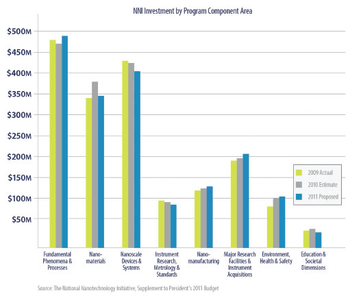
The mission of the National Nanotechnology Initiative (NNI) is to “provide a multi-faceted framework to assure U.S. leadership in nanotechnology that will be essential to improved human health, economic well being, and national security. The NNI invests in fundamental research to further understanding of nanoscale phenomena and facilitate technology transfer.” Since 2001, the NNI budget has grown from approximately $464 million, to the $1.8 billion budget currently proposed for 2011. This budget comes on top of the 2010 budget estimated to have been also approximately $1.8 billion, as well as an additional $511 million of funding for the NNI made available through the 2009 ARRA. Cumulatively, including the proposed 2011 budget, this totals over $14 billion of federal monies targeting nanotechnology since 2001.
To date, nanotechnology is proving to be instrumental in the development of new clean energy sources, its storage, transport, and conversion. Nanotechnology is also being used in filtration systems to purify water; specifically to remove arsenic from water. In general, nanotechnology offers innovative solutions to improve the environment.
The 2011 proposed federal budget supports this original mission, while shifting initiatives to accelerate the development of basic nanoscale research into real-life applications. In this endeavor, the supplement to the 2011 budget includes funding for three “signature” initiatives that represent the leading edge of functional interagency collaboration in the budget and program planning process under the NNI, with multiple agencies working in common toward specific objectives.
Nanotechnology Applications for Solar Energy: $51 million
The President’s agenda calls for the development of carbon-neutral alternative energy sources to mitigate global climate change, reduce dependence on foreign oil, improve the economy, and improve the environment. The development of a solar energy infrastructure is intended to support U.S. energy independence, while also representing an unparalleled economic opportunity if the U.S. can maintain scientific and industrial leadership in this field. Today, the current rate of improvement of solar technology performance is inadequate to meet future energy needs, and the cost is often not economically competitive without subsidies. Nanotechnology provides a key to overcoming current performance barriers and substantially improving the collection and conversion of solar energy. At the nanoscale, a number of physical phenomena have been identified that can improve the collection and conversion of solar energy. The goal of this initiative is to exploit the benefits of nanotechnology by enhancing understanding of conversion and storage phenomena at the nanoscale, improving nanoscale characterization of electronic properties, and helping enable economical nanomanufacturing.
Sustainable Nanomanufacturing – Creating Industries of the Future: $23 million
A long-term vision for nanomanufacturing is to create flexible, “bottom-up” batch assembly methods that can be used to assemble elaborate systems of complex nanodevices. The goal of this initiative is to accelerate during the next decade the development of industrial-scale methods for manufacturing of functional systems with relatively limited complexity based on manufactured nanoparticles with designed properties. The organized assemblies of nanoparticles manufactured will be designed to control and manipulate information, thermal energy, and electromagnetic radiation. The systems to be manufactured, based on these methods, will include disruptive technologies for high-speed communication and computation, solar energy harvesting, waste heat management and recovery, and energy storage. If the initiative is successful, the methods developed will be immediately extendable to more complex components and systems as future nanodevices mature.
Nanoelectronics for 2020 and Beyond: $55 million
Continuing to shrink the dimensions of electronic devices is essential to further increase processing speed, reduce device switching energy, increase system functionality, and reduce manufacturing cost per bit. But as the dimensions of critical elements of devices approach atomic size, quantum tunneling and other quantum effects degrade and ultimately prohibit conventional device operation. Approaches based on nanoscale science, engineering, and technology are the most promising for realizing the radical changes needed to overcome these fundamental physics limitations, and are expected to change the very nature of electronics and how devices are manufactured. Rapidly reinforcing domestic R&D successes in these arenas could establish a U.S. domestic manufacturing base that will dominate 21st-century electronics commerce. This initiative is intended to accelerate the discovery and use of nanoscale fabrication processes to produce revolutionary materials, devices, systems, and architectures to advance the field of nanoelectronics.
Targeted Federal Agencies
The largest share of the new budget is $424 million for the Department of Energy (DOE), coming on the heels of $293 million, over half, of the additional funding from the 2009 American Recovery and Reinvestment Act (ARRA) for NNI. This is approximately $50 million more than the estimated 2010 budget; reflecting the 2011 signature initiative for solar energy applications. The other growing budget is for the National Institutes of Health (NIH), receiving an additional $20 million approximately for biomedical advancements. (The FDA’s increased role in the NNI also reflects the great advances made in this area in the previous few years.) While these agencies are receiving more funding, the Department of Defense (DoD) is receiving less; and received none of the $511 million 2009 ARRA funding for NNI.
Environmental Health and Safety
As innovation continues and new nanoscale products and processes are developed, the federal government and others involved in nanotechnology recognize the need for balance between innovation and caution. The 2011 proposed budget supplement outlines funding for Environmental Health and Safety (EHS), including budgets for agencies not included in the NNI until this year: the Federal Drug Administration (FDA) and the Consumer Products Safety Commission (CPSC). In fact, although not the largest share of the budget, EHS funding is the fastest growing component of the NNI budget. Funding grew from $87 million in 2009 (including $12 million in ARRA funds) to a requested $117 million for 2011—triple the $35 million figure in 2005.
Nanotechnology In Education
In an effort to develop the next generation of scientists and engineers leading innovation in nanotechnology, two U.S. Senators introduced the “Promote Nanotechnology in Schools Act” (Bill S.3117) to help schools such as community colleges, universities, and even high schools purchase the advanced equipment needed to educate students and train workers in this emerging field. The bill is intended to help the U.S. maintain its leadership position by providing and better educating a skilled workforce that the NNI estimates will total two million trained workers within five years. The Act directs the National Science Foundation to establish a grant program that provides up to $400,000 to purchase nanotechnology equipment and materials to participating school, which will be required to provide matching funds of at least one-quarter the grant amount.
In The Pursuit of Nano
A decade into the National Nanotechnology Initiative, the United States has developed a leadership role. However, it is not the only country to recognize the tremendous economic potential of nanotechnology. While difficult to measure accurately, estimates from 2005 indicate that the European Union (EU) and Japan invested approximately $1.05 billion and $950 million, respectively, in nanotechnology. Behind them were Korea, China, and Taiwan with $300 million, $250 million, and $110 million respectively invested in nanotechnology research and development. The future will determine whether the U.S. maintains its leadership position and assists the world in developing new forms of clean energy, purification systems, materials, and industries that are cost-effective and safe.
Source URL: http://www.cemag.us/article/show-me-nano-money
McIlvaine Company,
Northfield, IL 60093-2743
Tel: 847-784-0012; Fax: 847-784-0061;
E-mail: editor@mcilvainecompany.com;
Web site: www.mcilvainecompany.com