OTHER ELECTRONICS

UPDATE


August 2006

McIlvaine Company


NANOTECHNOLOGY


An Internal Nanotechnology Task Force has been Formed

An internal nanotechnology task force has been formed by the FDA, says acting commissioner, Andrew C. von Eschenbach, M.D. The new task force is charged with determining regulatory approaches that encourage the continued development of innovative, safe, and effective FDA-regulated products that use nanotechnology materials.


Specifically, the task force will:


The task force is expected to submit its findings and recommendations to the acting commissioner by July 2007.


Nanotechnology Survey Results for the Use of Nanotechnology within the 2005 U.S. Manufacturing Industry


Background
In 2005, the National Science Foundation (NSF) awarded a grant to the National Center for Manufacturing Sciences (NCMS) to poll over 6,000 senior-level executives in leading U.S. organizations with leadership, technology or strategic research and development (R&D) responsibility to assess the outcome of growing private and public investments made in nano-technology under the National Nanotechnology Initiative (NNI). The overarching objective in conducting this largest known cross-industry benchmark study was to determine whether surveyed organizations treat nanotechnology differently from any other generation of advanced science and technology. The metric established by NSF was 300 survey responses to develop a credible profile – the survey netted 594 completed responses, representing a response rate of 10 percent.

Aggregate Observations
The NCMS survey of nearly 600 industry executives indicates that the state of the U.S. Nano-manufacturing Industry is generally vital, innovative and competitive for demonstrated passive nanotechnology products with many two-dimensional (2D) product applications growing rapidly for end-uses across diverse industry sectors. The survey confirms that the U.S. has the best-developed and mature research facilities, entrepreneurial culture and governance infrastructure for promoting new nanotechnology driven economic development.

Proliferation of Nanotechnology Start-ups
Besides the numerous entrepreneurial start-ups and small businesses (often led by researchers with academic or government laboratory connections), many larger manufacturers of conventional industrial materials and products as well as original equipment manufacturers (OEMs) and end-users, have begun to pursue internal research, actively seek new technologies, and partner in order to evaluate the potential for incorporating nanotechnology in differentiating their current product lines. Some of the world’s largest manufacturing organizations are actively developing their own pipelines and strategies for future products by adopting the specialized techniques to leverage risks and penetrate new markets with nanotechnology. Corporate partnering is critical for embryonic nanotechnology businesses to attain growth and viability; it begins anywhere from peer relationships to technology co-development and co-marketing, to culmination in merger and acquisition.

Diverse Nanotechnology Products in Development
Aggregate survey responses indicated that the U.S. Pacific region leads the Nation in development of diverse nanotechnology products and application markets that are being pursued for potentially disruptive economic, social, environmental and military advantage (Figure 1). Table 1 lists these applications.

AZoNano - The A to Z of Nanotechnology - Geographical distribution of 594 respondents corresponds closely with major public investments in nanotechnology

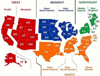
Figure 1. Geographical distribution of 594 respondents corresponds closely with major public investments in nanotechnology

Table 1a. Nanotechnology products and major application markets


Nano-tools, equipment logistics

Electronics & semiconductors

Computing, IT & telecoms

Aerospace

Automotive

Chemicals & processing

Nanotechnology Products


Semiconductors, nanowires, lithography & print products

X

X

X

X

X

X

Coatings, paints & thin films

X

X

X

X

X

X

Nanostructured particles, nanotubes & self assembly

X

X

X

X

X

X

Drugs delivery, diagnostics & implants

X

X

X


X

Nano-bio, nanofluidics & tissue engineering

X

X

X


Catalysis, battery, fuel cells & filtration

X


X

X

Environmental sensing & remediation

X

X


X

X

X

Defence, security & protection

X

X


X

X


Electronic devices, displays & optoelectronics

X

X

X

X

X


Nano-manipulation, visualization, biomarkers & Q-dots

X

X

X


X

Computing, design, imaging tools, & products


X

X


Personal care, nanofluids & colloids


X

Convergence products (Nano-bio-IT-cognitive)


X


Other


Table 1b. Nanotechnology products and major application markets


Sensing, environmental & security

Energy & utilities

Fabricated products

Consumer products & textiles

Pharma, biomedical & biotech

Off highway & transportation

Nanotechnology Products


Semiconductors, nanowires, lithography & print products

X

X

X

X

X


Coatings, paints & thin films

X

X

X

X

X

X

Nanostructured particles, nanotubes & self assembly

X

X

X

X

X

X

Drugs delivery, diagnostics & implants

X


X

X

X


Nano-bio, nanofluidics & tissue engineering

X


X

X

X


Catalysis, battery, fuel cells & filtration

X

X

X

X

X

X

Environmental sensing & remediation

X

X

X

X

X

X

Defence, security & protection

X

X

X

X

X


Electronic devices, displays & optoelectronics

X

X

X

X

X


Nano-manipulation, visualization, biomarkers & Q-dots

X


X

X

X


Computing, design, imaging tools, & products


Personal care, nanofluids & colloids


X

X


Convergence products (Nano-bio-IT-cognitive)


X


Other


Table 1c. Nanotechnology products and major application markets


Machine tools & machinery

Housing & construction

Food & agriculture

Metals, mining & material production

Nanotechnology Products


Semiconductors, nanowires, lithography & print products

X


X

Coatings, paints & thin films

X

X

X

X

Nanostructured particles, nanotubes & self assembly

X


X

X

Drugs delivery, diagnostics & implants


X


Nano-bio, nanofluidics & tissue engineering


X


Catalysis, battery, fuel cells & filtration


X

X

Environmental sensing & remediation


X

X

Defence, security & protection


X

Electronic devices, displays & optoelectronics


X


Nano-manipulation, visualization, biomarkers & Q-dots

X


X

X

Computing, design, imaging tools, & products


Personal care, nanofluids & colloids


X

X

Convergence products (Nano-bio-IT-cognitive)


Other


X


The U.S. leads the world in the generation and commercialization of nanoscale materials, manipulation tools and measurement innovations being applied to initially benefit a growing range of consumer products, digital storage, photovoltaic and semiconductor manufacturing industries. Myriad new applications of advanced nanocoatings, nanofilms and nanoparticles are being developed for introduction in the near-term (3-5 years) on a broader range of durable goods, consumer electronics and medical products (Figure 2). Nanoproduct applications are also being developed for the next generation semiconductor, energy, chemical catalysis and pharmaceutical/biomedical products. These would eventually mature into convergence products with higher sensory complexity, self-assembly and autonomous functionality, offering greater potentials for achieving the envisioned economic and societal impact.


AZoNano - The A to Z of Nanotechnology - Commercialization timelines indicate many new nanoproducts introductions in 2007-2011

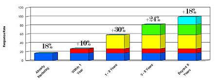
Figure 2. Commercialization timelines indicate many new nanoproducts introductions in 2007-2011

Few Early Successes, Many Barriers
Organizations are proceeding cautiously in the development and commercialization of innovations such as active three-dimensional (3D) nanotechnology products that involve more direct human, societal and environmental impact. The nano-manufacturing industry for second generation (potentially disruptive) nanotechnology products is largely in its infancy – there are as yet no commercial devices based on true nanotechnology. The challenges facing the industry are not limited to the technology itself – rather, factors such as funding, commercialization strategies, regulation and a variety of socio-business issues will affect the long-term success of organizations entering this domain.

Due to the cross-disciplinary nature and broad societal implications of nanotechnology, few organizations possess the vertical integration and expertise needed to rapidly commercialize the envisioned second generation nano-products from conception to consumption. While there is much exploratory partnering and co-development within the industry, it will accelerate when the early nanotechnology applications transcending lengths of scale are able to demonstrate unquestionably superior performance of existing macro-scale products and systems at affordable cost, improved margins and higher reliability.


Large-scale, market-driven investments have been somewhat inhibited due to the lack of broader, in-depth understanding of nanotechnology’s complex material-process-property phenomena and its interactions with humans and the environment. These issues uphold the perception of uncertainty and long lead times in the industry. Therefore, the near-term impact of nanotechnology is likely to be fragmented, product-specific and evolutionary rather than revolutionary. The distillation of survey trends and executive attitudes indicates that while new applications will grow in the near-term largely by entrepreneurial means (e.g. technology push to seek niche applications), the longer-term success of a nano-manufacturing venture would depend on an organization’s core competency to partner with end-users and technology providers on the basis of platform nanotechnologies as well as its ability to meet defined performance object-tives (i.e. market pull factors) that help meet the customers’ bottom-line.

Increased Corporate and Public Awareness
Traditional manufacturing organizations, while interested in adopting nanotechnology, tend to be preoccupied with issues of short-term profitability and other approaches that prioritize returns and revenues over long-term growth (such as innovation and skills development). Recent pronouncements of the importance of nanotechnology herald a significant change in corporate and National attitudes. For prepared organizations, these trends represent new opportunity for paradigm shifts in change management to drive innovations for superior product lines, and realize improved investment returns on a global scale.

These positive trends are attributed in large part to the substantial seed investments, leadership and outreach efforts made by the NNI through R&D undertaken across academia, small and large businesses and the National Laboratory infrastructure. Concurrently, the increased branding of leading-edge consumer products and coining of science fiction terms with “nano” have also raised societal awareness, albeit with mixed results. They have the longer-term impact of preparing both, a new generation of know-ledge workers and informed consumers.


Survey respondents unanimously indicated that sustained government sponsorship is essential to attract the attention of senior manufacturing industry executives, investors, media and the public. Government support will expedite improved fundamental understanding of nano-technology and further clarify its potential, while fostering both, early markets and entrepreneurship towards the more advanced generation product applications.

Addressing Key Industry Barriers
The majority of the surveyed executives indicated their organizations faced considerable difficulty in nano-manufacturing, ranging from emergent technology issues, to raising capital for critical infrastructure investments, attracting the technical and business talent, connecting with early end-users, and producing competitively to meet new market applications and volumes.

Intellectual property (IP) issues and the sharing of knowledge were identified as areas of significant concern, as well as the lack of clear regulatory policy, which could impede industry, and impact the public’s reaction to future product developments. The continued education of the public, policymakers (State and Federal), government agencies and legislative bodies regarding these issues will result in clearer product approval pathways, robust standards and responsible practices, and thereby help ensure the continued dominance of the U.S.


While the nano-manufacturing industry faces unique challenges, similarities do exist with other recent technology waves such as the Internet and biotechnology, offering many lessons learned for formulation of sound anticipatory approaches. The answers to addressing the top-ranked challenges lie in continuing the aggressive National R&D investment policies for pursuing targeted investigations in fundamental nano-scale science, engineering and manufacturing technology. NCMS recommends several approaches for addressing the technology and business needs of the U.S. Nano-manufacturing Industry, while responsibly accelerating the benefits of new or enhanced products for societal benefit. NCMS further recommends the reclassification of the conventional definition of “small” business, as many of the largest organizations working with nanotechnologies would be considered small businesses by traditional industry standards. The following three broad categories are suggested in addressing the unique needs of current generation of embryonic nanotechnology businesses:

  • Small nanotechnology businesses (less than 20 staff)

  • Medium nanotechnology businesses (21 – 100 staff)

  • Large nanotechnology businesses (over 100 staff).

Table 2 lists several approaches and National strategies for addressing clusters of identified barriers to the nano-manufacturing industry.


Table 2. Strategies to address critical identified barriers faced by the U.S. Nano-manufacturing industry

Industry Barriers

Recommendations

High cost of processing

Process scalability issues

Lack of development tools

Collaborative R&D in value-chains

R&D to reduce/combine process steps

R&D in new equipment and to improve product yields

Long time-to-market

Unclear societal benefits

Government incentives for private R&D investments

Raise public awareness of benefits via successes

Promote supplier/end-user partnerships

Insufficient investment capital

Government investment in pre-competitive R&D

Stimulate market pull via end-users

Mentor start-ups for attracting investment

Intellectual Property (IP) issues

New business models for nanotech value-chains

Legal reform, train legal and judicial professionals

Streamline partnering with academia and National Labs

Facilitate supplier/end-user partnerships

Shortage of qualified manpower/

Multi-disciplinary aspects

Retrain tech workforce in basic science/testing/quality

Attract students to science and engineering careers

Regulatory and safety concerns/

Environmental and toxicity issues

Streamline permit/product approvals at agencies

Increase government-sponsored R&D

Broader dissemination of findings

Balanced legislation and regulatory practices

Accelerating Nanotechnology Developments
In order to maintain the current high momentum of innovation in nanotechnology advances critical investment, business and regulation-related issues need to be addressed concurrently and collaboratively by State and Federal policymakers. Long-term policies for National investment and the stimulation of public-private-research partnerships are imperative for developing the fundamental science base, facilitating technology transition to applied research, and demonstrating credible nanotechnology-enabled applications that are perceived as meaningful to our quality of life. The potential risks and hazards associated with the more revolutionary envisioned nanotechnology applications need to be assessed and disseminated by trusted sources to raise the public’s awareness, and thereby gain societal confidence. Strong incentives will help resulting innovations become swiftly translated into industry led technology demonstrations that enhance the public’s awareness and acceptance. This will require dramatic changes in business strategy and unprecedented levels of public-private regulatory collaborations to responsibly commercialize future nano-product applications. Such levels of integration do not presently exist.

Public-Private Collaborations
It is unlikely that the vast field of nanotechnology would reach the levels of maturity (like other traditional physical science-based industries did) within our lifetimes. This justifies the case for long-term government investment in nanotechnology. Private and institutional investments would grow faster when some of the fundamental technical issues of process scalability and cost of production of new nano-components as well as associated risks have been more comprehensively addressed.

Public-private collaborations in applied nanotechnology will hasten societal support when targeted towards nearer-term national concerns such as:

·                    Increasing productivity and profitability in manufacturing

·                    Improving energy resources and utilization

·                    Reducing environmental impact

·                    Enhancing healthcare with better pharmaceuticals

·                    Improving agriculture and food production

·                    Expanding the capabilities of computational and information technologies.

Critical Role of Government
Government can lead by defining and funding National priorities, and creating meaningful grand challenge incentives for early industrial adopters of nanotechnology. This will accelerate the broad-based translation of nanotechnology advances across multiple industry sectors.

Areas where greater government involvement in nanotechnology can have high National impact while leveraging substantially larger private investments include:

·                    Incentives favoring longer-term investments (e.g. tax-free bonds for financing, tax credits for capital investments, reduced capital gains tax rates, investment-specific loan guarantees, etc.)

·                    Promoting and streamlining strategic alliances for businesses and researchers with larger players or end-users

·                    Providing mentorship and business planning assistance to small businesses to identify key technology benefits and attract private capital

·                    Underwriting and disseminating “good science” research and public education into the long-term issues related to waste disposal, safety and regulations

·                    Undertaking tort and legal reform which will provide developers greater immunity and protection once their products are federally approved.

State governments and economic development bodies could assist small and large businesses link up in “ecosystem-like” neutral development environments by promoting leverage of nano-incubator and user facilities. By working with university and National Laboratory technology transfer organizations, they could facilitate simpler access to nanotechnology resources and training available in educational institutions, thereby stimulating new partnerships with entrepreneurs. Offering matching funds and other seed incentives to organizations pursuing Federal nanotechnology programs would provide further impetus for businesses and researchers to partner in commercialization ventures. Several progressive U.S. States have already initiated these next-generation technology partnerships.


OTHER ELECTRONICS


Q2 IC Industry Output up 33.6 Percent on One Year Ago

Taiwan's IC industry production reached NT$337.1 billion (US$10.25 billion) in the second quarter of this year, up 33.6 percent over the same period last year and 9.8 percent from the previous quarter, according to a government think tank.


The Ministry of Economic Affairs' Industrial Technology Research Institute (ITRI) forecast that third-quarter output will grow to NT$350.8 billion and annual output will top NT$1.3633 trillion (US$41.44 billion) in 2006, an increase of 22 percent from 2005.


According to Peng Mao-jung, an ITRI analyst, since the second quarter is traditionally a slack season for IC designing and is affected by a slower market demand for TFT displays and an oversupply of LCD-driven ICs, most IC-designing companies did not register a strong performance during the season.


However, small LCD-driven IC-designing companies were little affected, recording better sales than during the previous season, he pointed out.


Sales of consumer electronic products turned brisk in May, with IC makers also enjoying good business, enabling IC designers to score a production value of NT$77.5 billion in the second quarter, an increase of 6.5 percent from the previous quarter and 19.8 percent over the same time last year, Peng said.


IC manufacturing faced a similar situation, churning out an output in the second quarter -- traditionally a slack season -- that was 12.5 percent higher than the previous quarter.Contract chip-making accounted for 5.5 percent of IC manufacturing output.


Taiwan Semiconductor Manufacturing Corp. (TSMC), the world's largest contract-chip maker, reported a 5.5 percent growth in the second quarter over the first, and a yearly growth of 36.9 percent.


United Microelectronics Corp. (UMC), another of the world's leading contract-chip makers, scored similar seasonal and yearly growths for the second quarter — 5.6 percent and 32.4 percent, respectively. Profit margins improved and the utilization of its production capability rose to 80 percent, up slightly from the first quarter, according to ITRI.


DRAM business has been the main driving force behind the substantive growth in Taiwan's IC manufacturing industry in the second quarter of 2006, Peng said.


He attributed this to improved production capability and yield of the DRAM business's 12-inch wafer plants, as well as their improved production technologies.


Internationally, major DRAM makers switched some of their production facilities to producing NAND Flash, bringing down the supply of DRAM chips and raising DDR and DDR2 prices, according to the analyst.


He said Taiwan's IC manufacturers produced a total of NT$183.9 billion in products during the second quarter of 2006, a whopping growth of 40.8 percent from the same period in 2005.


As for the testing and packaging business, he said the second quarter output registered only single-digit growth from the first quarter, influenced by the slow recovery in the personal computer (PC) market. Still, the output figure represented a double-digit growth from the same time last year, he added.


The less impressive performance of Taiwan's testing and packaging business was also due to Microsoft Corp.'s decision to delay marketing of the new Vista operating system which affected sales of PCs and peripherals. Slow sales of low-end cellphones also cooled the demand in testing and packaging of low-end communications chips.


As a whole, the utilization of the testing and packaging business's capabilities went down to 80 percent in the second quarter, but is expected to pick up in the third quarter as PC sales are anticipated to rise when the academic semester begins in September.


For the second quarter, Taiwan's IC-packaging business registered an output of NT$52.3 billion, up 6.7 percent from the previous quarter and 27.6 percent year-on-year, with the IC-testing business registering an output of NT$23.4 billion for a quarterly and yearly growth of 7.8 percent and 45.3 percent.


The ITRI forecast that Taiwan's overall IC industry output will reach NT$350.8 billion in the third quarter, up 4.1 percent from the second, and that 2006 output will reach NT$1,363.3 billion -- a 22-percent increase over 2005.


Taiwanese IT Manufacturers Detected Not Compliant with RoHS

Test and analysis lab Integrated Service Technology (IST) estimated around four to five listed Taiwanese electronics companies have been caught disqualified for RoHS (Restriction of Hazardous Substance) directive and fined for the failures.


The European Union (EU) put the directive into effect beginning July 1 this year. The test company pointed out these disputed companies were each fined over NT$10 million (US$312,500 at US$1:NT$32) and one of them even faced NT$100 million (US$3.1 million) worth of merchandise returned for poor performance in its lead-free products.

However, the Ministry of Economic Affairs said it has not received any information on the reported cases.


IST's executives pointed out that many Taiwanese have overlooked the impact of RoHS before RoHS was in position. They noted a large number of error analysis contracts have swarmed their company, suggesting that Taiwanese manufacturers were facing real challenge from RoHS.


The company's executives added that Taiwanese manufacturers have not heeded lurking unreliability resulting from lead-free process when they were busy shifting to the process.

The reported disqualified cases put a damper on a government data released in late June this year. The data showed over 90 percent of Taiwan's products bound for Europe were already RoHS compliant.


However, some Taiwanese electronics manufacturers have benefited from the directive, the test company said. They include copper clad laminate maker ITEQ Corp., LED maker Arima Optoelectronics Corp., and silicon foundry United Microelectronics Corp.


IST is currently Taiwan's largest provider of test and analysis on ecological electronics, commanding around 80 percent of the domestic market.


Researchers Partner on 'first' MEMS Integrated on CMOS

 According to R. Colin Johnson, Advanced Diamond Technologies Inc. (ADT), a spin-off from the U.S. Energy Department's Argonne National Laboratory, partnered recently with microelectromechanical systems (MEMS) pioneer Innovative Micro Technology and the University of Wisconsin at Madison. They will supply the Defence Advanced Research Projects Agency (Darpa) with RF MEMS oscillators and resonators by next year as these institutions co-develop the world's first MEMS directly integrated onto a CMOS chip.


MEMS devices will be integrated with CMOS chips using the ultrananocrystalline diamond thin films patented by Argonne National Laboratory and licensed to ADT. Low-temperature processing required for diamond films enables MEMS circuit components to be fabricated in pre-designated areas on finished CMOS chips.


"We call our process MEMS-on-CMOS because, today, if you want to add a MEMS device to your CMOS chip, you have to make two chips—one CMOS and one MEMS—and bond them together," said ADT President Neil Kane. "We can add diamond MEMS devices to any CMOS chip while it's being fabricated." The Darpa Phase II program is being funded at Rs.6.50 crore ($1.4 million) for one year. The partners will then deliver prototype chips with a MEMS resonator and oscillator fabricated alongside CMOS circuitry. The Wisconsin researchers will use atomic force microscopy tools to characterize the MEMS device's performance. According to the press release, if the prototype proves successful, Darpa would likely fund a third and final phase.


The prototype device will aim for a modest 100MHz benchmark, but MEMS oscillators made from ultrananocrystalline diamond should be able reach 3GHz within a few years, according to ADT CTO John Carlisle.


Carlisle said commercialization of diamond is also being driven by cost since it is cheaper. The technique could also help designers add venerable quartz crystal oscillators that sell for 50 cents directly to chips.


Hon Hai Remains No.1 Taiwanese Electronics Manufacturer

In July 2006, Hon Hai Precision Industry Co., Ltd. raked in revenue US$2.1-billion retaining the No.1 notch on Taiwan's top 10 electronics manufacturer rating.


Asustek finished second on the rating, with consolidated revenue of US$1.48-billion, up 74.3 percent from year-earlier period. Asustek delivered 4.05 million motherboards in July, losing 4 percent from June. However, average selling price of the board surged. Its July shipment of notebook computers stayed on par with the June level, numbered at 450,000 to 500,000 systems. But the shipment for July jumped 70-80 percent from the same period of last year.  Throughout the first seven months this year, the company had shipped 2.5-2.5 million boards, increasing 40 percent year-on-year.


Quanta Computer was ranked the third largest player on the rating, reporting revenue of US$1-billion in July. Meeting expectations, the result was down 16.2 percent from a month earlier whereas inching up 0.39 percent from the same period of last year. Its cumulative revenue in the first seven months this year was US$7.4 million, surging 19.79 percent year-on-year.

Institutional investors estimated Quanta Computer shipped 1.45 million notebook computers last month, slipping from June. However, the company expected the shipment to begin returning to 1.7 million systems in August.


Taiwan Semiconductor Manufacturing Co. (TSMC) reported revenue of US$873-million in July, increasing 1.1 percent from a month earlier. The result made it the fourth-largest player on the rating.


Compal Electronics scored revenue of US$864-million last month, making it the No. 5 player. The result was up 22.3 percent from a year earlier and 41.67 percent from the comparable period of last year. Its cumulative revenue for the first seven months was US$4.6-billion, increasing 21.98 percent from a year earlier. The company delivered 1.25 million notebook computers in July alone, a gain of over 20 percent from a month earlier.


Acer was the sixth-leading player on the rating last month, with revenue of US$774-million, increasing 10.8 percent year-on-year whereas down 9.4 percent from June.


AU Optronics (AUO) snatched up the seventh post in July, with revenue topping US$628-million, up 15.38 percent from the same month of last year. Inventec Corp. held the eighth post, with revenue of US$572-million. Wistron was the ninth-leading player, with revenue of US$546 million. BenQ came last with consolidated revenue of US$509-million.


Taiwan Science Parks to Generate NT$2-Trillion Sales in 2006

Taiwan science parks including Hsinchu Science Park (HSP), Central Taiwan Science-based Industrial Park (CTSP) and Southern Taiwan Science Park (STSP) reported revenues of NT$825 billion in the first half of this year, according to today's Chinese-language Economic Daily News (EDN), citing the latest report from Taiwan's National Science Council. CTSP saw a 198 percent on year growth amid strong growth in Taiwan's TFT LCD industry.


The three science parks are expected to have revenues of NT$2 trillion in 2006, the paper noted.


Taiwan Science Parks, 1H06 Revenues (NT$ Billion)


Name


1H06

Y/Y Growth


2006(f)

Number of Companies

Number of Employees

HSP

540

21%

1,200

385

116,349

CTSP

70.557

198%

120-180

80

10,455

STSP

211.97

50.7%

500

187

44,749


Source: National Science Council as cited in EDN, compiled by DigiTimes, August 2006


The European Commission Endorsed Aid to Poland

The European Commission has endorsed aid to Poland for a grant to eight Korean-based companies to set up a cluster of nice electronics projects in Kobeirzyce, Poland.  The companies in the cluster will manufacture liquid crystal display TV modules, related componets as well as down stream products.   The cluster comprises these investments:


The total eligible cost of the nine investment projects amount to €711.1 million.  The investments would occur between 2006 and 2011. 


China Video Industry Association Agrees to Promote and Support HDMI

Silicon Image, Inc., a leader in semiconductors for the secure storage, distribution and presentation of high-definition content announced a landmark agreement with the China Video Industry Association (CVIA) under which CVIA will promote and support the use of High-Definition Multimedia Interface (HDMI) by the consumer electronics industry in China. The agreement with CVIA positions China to play a major role developing next-generation digital consumer electronics technology.


As part of the agreement, Silicon Image and CVIA have agreed to work together to promote HDMI adoption among domestic Chinese electronics manufacturers, co-develop new technology applicable to HDMI, and collaborate on establishing testing and interoperability certification labs that complement the capabilities of the HDMI Authorized Testing Centers established by Silicon Image.


In addition, Silicon Image will support the China Digital Interface Industry Alliance (CDIA), an industry alliance consisting of major Chinese electronics manufacturers that CVIA is establishing. CDIA will work to promote the use of HDMI in consumer electronic products, promote communications among manufacturers in China and abroad, and strengthen coordination between hardware manufacturers and content providers.


In 2005, China manufactured 82 million televisions and 140 million DVD or VCD players, according to CVIA. Sales of plasma and LCD TVs are forecast to grow 105 percent this year to $5.5 billion, and are estimated to reach $10.5 billion in 2008, according to IDC.


"Today China is taking a major step forward in promoting the development of its digital consumer electronics industry," said Bai Weimin, director of the Department of Broadcasting and Television, Ministry of Information Industry. "CVIA's agreement to partner with Silicon Image to develop new digital interface technology will further the development of China's electronics manufacturers as leaders in creating advanced digital technologies."


"Under this agreement, China's companies will not only embrace the global HDMI standard but will partner with Silicon Image to participate in future technology development for HDMI," said Hao Yabin, vice secretary-general of the China Video Industry Association. "This agreement will help China develop its own intellectual property, protect the interests of China's digital consumer electronics industry, and improve the cooperation and mutual benefit of the domestic and international high definition technology industries."


New Testing Labs

As part of the agreement, Silicon Image and CVIA will cooperate in establishing testing and interoperability certification labs. Silicon Image will continue to operate HDMI Authorized Testing Centers (ATCs) and Simplay HD Testing Centers in China. In addition, Silicon Image, through its wholly-owned subsidiary, Simplay Labs, LLC, and CVIA will work together to establish testing and interoperability certification labs that complement the capabilities of the HDMI ATCs.


Silicon Image also announced the opening of China's second combined HDMI ATC / Simplay HD Testing Center in Shanghai, and with the support of CVIA plans to open a third such facility in China at a location to be determined.


The Simplay HD Testing Program consists of branding, compatibility testing, and education for consumers to provide them with a consistent "plug and play" user experience and to maximize their access to premium high definition (HD) content.